Organic light-emitting device, manufacturing method thereof, and display method

A technology of electroluminescent devices and manufacturing methods, which is applied in the fields of organic semiconductor devices, electric solid devices, semiconductor/solid device manufacturing, etc., and can solve problems such as difficulty in entering the light-emitting layer, poor energy level matching of the light-emitting layer, and low luminous efficiency of light-emitting devices, etc. question

Active Publication Date: 2015-11-18
BOE TECH GRP CO LTD
View PDF10 Cites 11 Cited by
  • Summary
  • Abstract
  • Description
  • Claims
  • Application Information

AI Technical Summary

Problems solved by technology

[0004] However, during the research and development process, the inventors of the present application found that the energy level of the material that can be used to form the hole transport layer through the solution process is poorly matched with the energy level of the light-emitting layer, so that the holes in the hole transport layer It is difficult for carriers to enter the light-emitting layer, resulting in low luminous efficiency of organic electroluminescent devices

Method used


Image

  • Organic light-emitting device, manufacturing method thereof, and display method
  • Organic light-emitting device, manufacturing method thereof, and display method
  • Organic light-emitting device, manufacturing method thereof, and display method

Examples


Embodiment 1

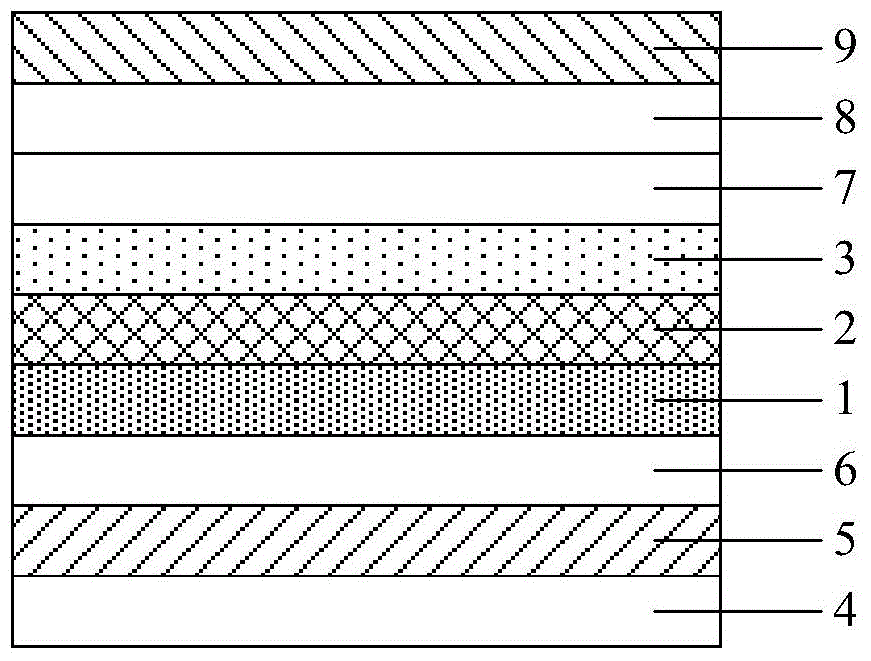
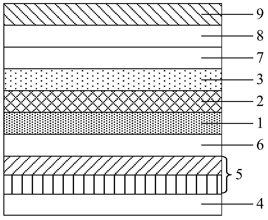
[0048] An embodiment of the present invention provides an organic electroluminescent device, specifically, such as figure 1 As shown, the organic electroluminescence device comprises a hole transport layer 1, a light emitting layer 3 and an interface modification layer 2 between the hole transport layer 1 and the light emitting layer 3, and the material of the interface modification layer 2 is a material having hole transport ability material, that is, the interface modification layer 2 can transport hole carriers, and the energy level of the interface modification layer 2 is between the energy level of the hole transport layer 1 and the energy level of the light-emitting layer 3, so that the interface modification layer 2 The energy level matching between the hole transport layer 1 and the light-emitting layer 3 is good, so that the hole carriers in the hole transport layer 1 can easily enter the light-emitting layer 3, thereby effectively improving the organic electroluminesc...

Embodiment 2

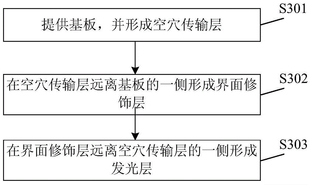
[0081] In addition, an embodiment of the present invention provides a method for manufacturing the organic electroluminescent device described in Embodiment 1, specifically, as image 3 As shown, the fabrication method of the organic electroluminescent device comprises:

[0082] Step S301 , providing a substrate, and forming a hole transport layer.

[0083] Step S302, forming an interface modification layer on the side of the hole transport layer away from the substrate.

[0084] Step S303, forming a light emitting layer on the side of the interface modification layer away from the hole transport layer.

[0085] Wherein, the material of the interface modification layer includes a material with hole transport capability, and the energy level of the interface modification layer is between the energy level of the hole transport layer and the energy level of the light emitting layer.

[0086] Since the electroluminescent device manufactured by the above method includes an interf...


PUM


Abstract

The invention discloses an organic light-emitting device (OLED), a manufacturing method thereof, and a display method, and relates to the technical field of display. The luminous efficiency of the OLED can be improved. The OLED comprises a hole transport layer, a light-emitting layer, and an interface modification layer arranged between the hole transport layer and the light-emitting layer. The material interface modification layer comprises a material having a hole transporting capability. The energy level of the interface modification layer is between that of the hole transport layer and that of the light-emitting layer.

Description

technical field [0001] The invention relates to the field of display technology, in particular to an organic electroluminescence device, a manufacturing method thereof, and a display device. Background technique [0002] An organic light-emitting device (Organic Light-Emitting Device, referred to as OLED) is a device that uses electro-excited phosphors or phosphor organic compounds to emit light. Organic electroluminescent devices have great application prospects in the display field because of their many advantages such as self-luminescence, all-solid-state, wide viewing angle, and fast response. [0003] In existing organic electroluminescent devices, organic electroluminescent devices usually include a substrate, a bottom electrode, a hole injection layer, a hole transport layer, a light emitting layer, an electron transport layer, an electron injection layer and a top electrode stacked in sequence. ; Wherein, the material of the hole transport layer is a solution-type m...

Claims


Application Information

Patent Timeline
Patent Type & Authority Applications(China)
IPC IPC(8): H01L51/50H01L51/54H01L51/56
CPCH10K85/113H10K50/156H10K71/00H10K50/826H10K2102/3026H10K50/11H10K50/818H10K50/828H10K85/111H10K85/115H10K85/342H10K85/622H10K85/623H10K85/626H10K85/633H10K85/1135H10K85/6572H10K2101/40H10K2101/30
Inventor 廖金龙
Owner BOE TECH GRP CO LTD
Why Eureka
Try Eureka