Dielectric dual-mode bandpass filter based on patch structure
A filter and dielectric resonator technology, applied in waveguide-type devices, electrical components, circuits, etc., can solve the problems of limited method and structure realization performance, difficult processing technology, complex structure, etc., to achieve simple structure and reduce processing. Difficulty, the effect of high out-of-band rejection
- Summary
- Abstract
- Description
- Claims
- Application Information
AI Technical Summary
Problems solved by technology
Method used
Image
Examples
Embodiment 1
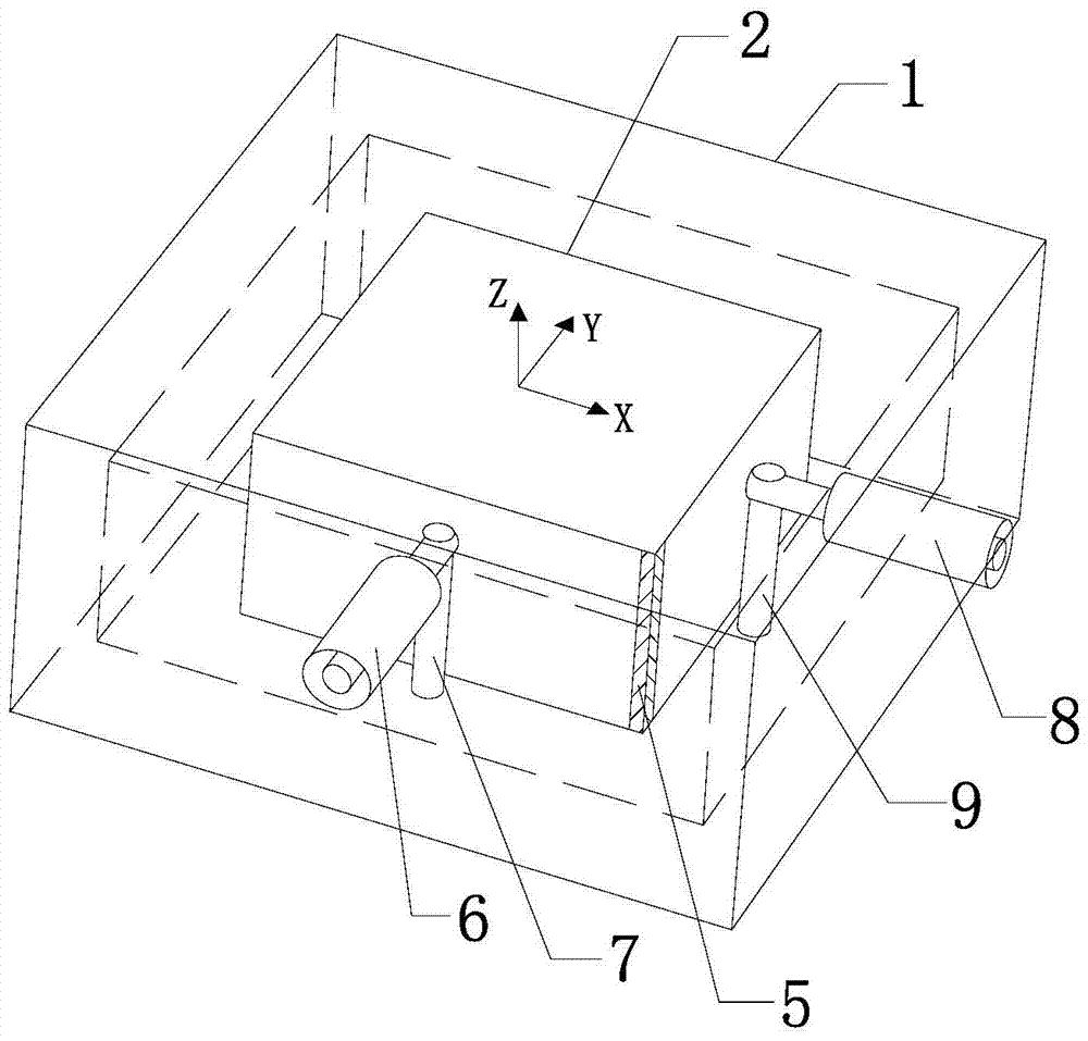
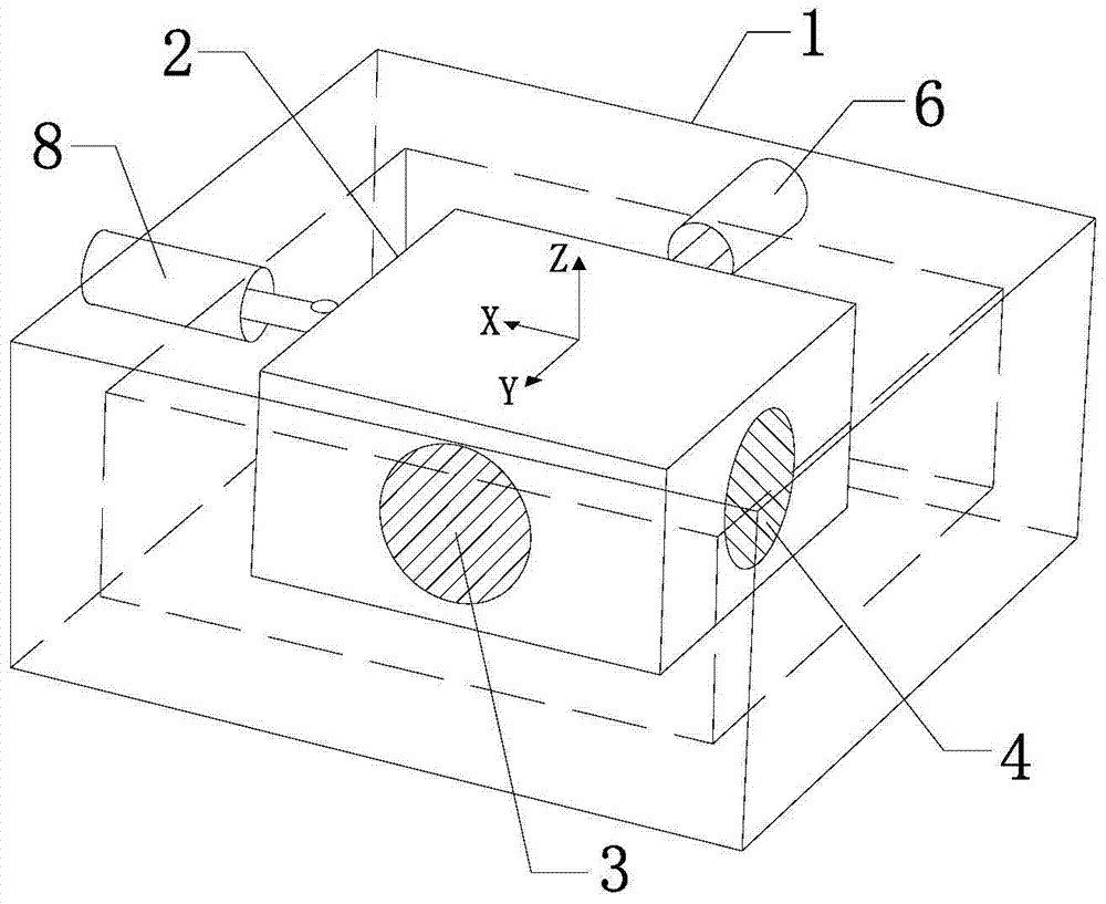
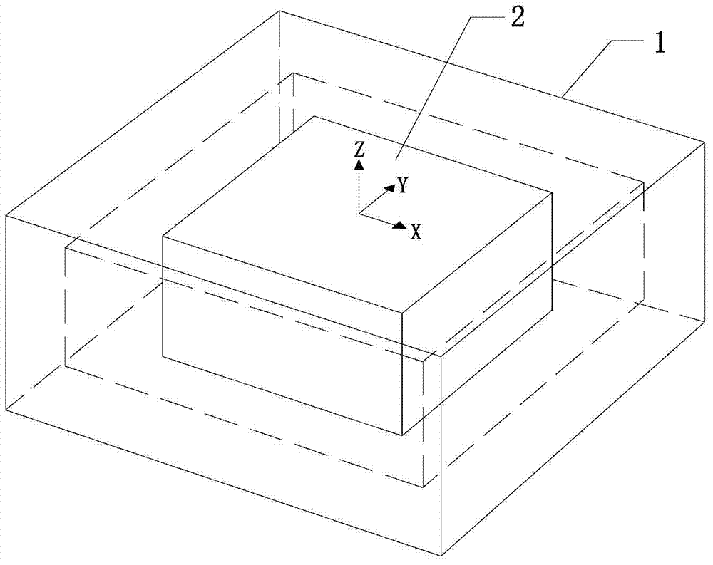
[0058] Such as figure 1 with figure 2 As shown, the dielectric dual-mode bandpass filter of this embodiment includes a cavity 1, the cavity 1 is a rectangular cavity with a size of 30mm*30mm*10mm, and a dielectric resonator 2 is placed in the center of the cavity 1 , the upper and lower ends of the dielectric resonator 2 are connected to the cavity 1, and the two degenerate modes (ie, resonance modes) adopted by the dielectric resonator 2 are called TM120 mode and TM210 mode;
[0059] The dielectric resonator 2 is a rectangular dielectric resonator with a size of 20mm*20mm*10mm and a dielectric relative permittivity of 21.4. On the two adjacent outer surfaces of the dielectric resonator 2 (in this embodiment, the two outer surfaces The first metal patch 3 and the second metal patch 4 are pasted on the side (rear side and left side), and it can be seen that the transverse centerline of the first metal patch 3 and the transverse centerline of the second metal patch 4 Vertical...
Embodiment 2
[0072] This embodiment is based on the dielectric dual-mode bandpass filter of the two above-mentioned embodiment 1, utilizing such as Figure 15 (S in the figure represents the source end, L represents the load end, and 1 to 4 represent modes 1 to 4, respectively) The fourth-order linear topology shown in the figure can design a linear topology dual-mode dual-cavity dielectric bandpass filter, such as Figure 16 As shown, the coupling method of mode 2 and mode 3 is to achieve mode coupling through a closed metal ring, and the size of the metal ring (width ring_w, height ring_h) controls the size of the coupling coefficient, such as Figure 17 Shown; The S-parameter response of the linear topology dual-mode dual-cavity dielectric bandpass filter is as follows Figure 18 It can be seen from the figure that, in the bandwidth of 2634MHz-2698MHz, the passband return loss is below -15.6dB.
Embodiment 3
[0074]This embodiment is based on the dielectric dual-mode bandpass filter of four above-mentioned embodiment 1, utilize Figure 19 (S in the figure represents the source end, L represents the load end, and 1 to 8 represent modes 1 to 8 respectively) The eighth-order linear topology shown in the figure can design a linear topology dual-mode four-cavity dielectric bandpass filter, such as Figure 20 As shown, the coupling mode of mode 2 and mode 3, mode 4 and mode 5, mode 6 and mode 7 is to achieve mode coupling through a closed metal ring, and the size of the metal ring controls the size of the coupling coefficient; the linear topology dual-mode four-cavity medium The S-parameter response of the bandpass filter is as Figure 21 It can be seen from the figure that, in the bandwidth of 2632MHz-2699MHz, the passband return loss is below -12.2dB.
PUM
 Abstract
Description
Claims
Application Information


