Reaction cavity and semiconductor processing equipment

A reaction chamber and cavity technology, applied in metal material coating process, gaseous chemical plating, coating and other directions, can solve the problems of poor film quality, uneven airflow, inconvenient maintenance, etc., and achieve convenient cleaning. And maintenance, improve film quality, the effect of fast entry

Active Publication Date: 2015-11-25
HUNAN RED SUN PHOTOELECTRICITY SCI & TECH
View PDF5 Cites 4 Cited by
  • Summary
  • Abstract
  • Description
  • Claims
  • Application Information

AI Technical Summary

Problems solved by technology

There are problems such as complex structure, difficult processing, high processing cost, and inconvenient maintenance. In addition, the process gas enters from the top and enters the chamber from the bottom of the chamber after passing through a certain channel. The speed of process gas entering the reaction chamber is slow, which is easy to cause airflow Uneven, poor film quality, etc.

Method used


Image

  • Reaction cavity and semiconductor processing equipment
  • Reaction cavity and semiconductor processing equipment
  • Reaction cavity and semiconductor processing equipment

Examples


Embodiment Construction

[0024] The present invention will be described in further detail below in conjunction with the accompanying drawings and specific embodiments.

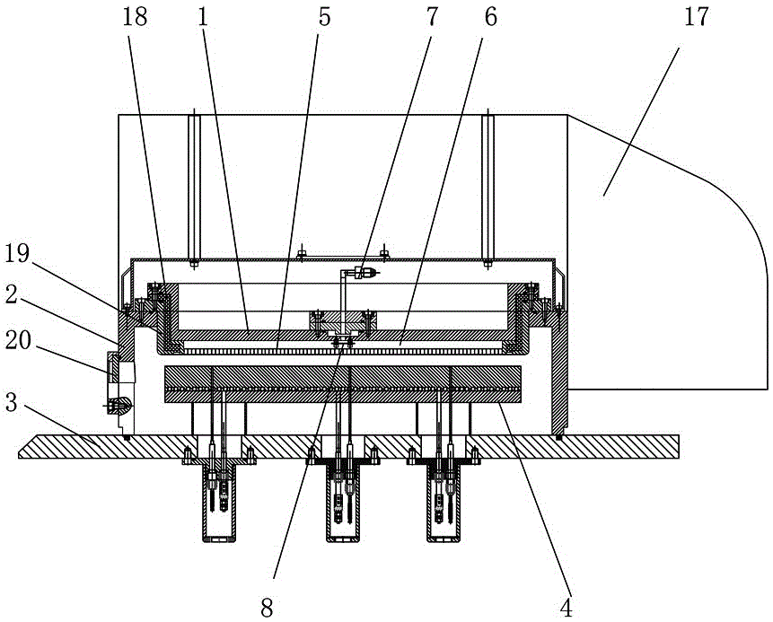
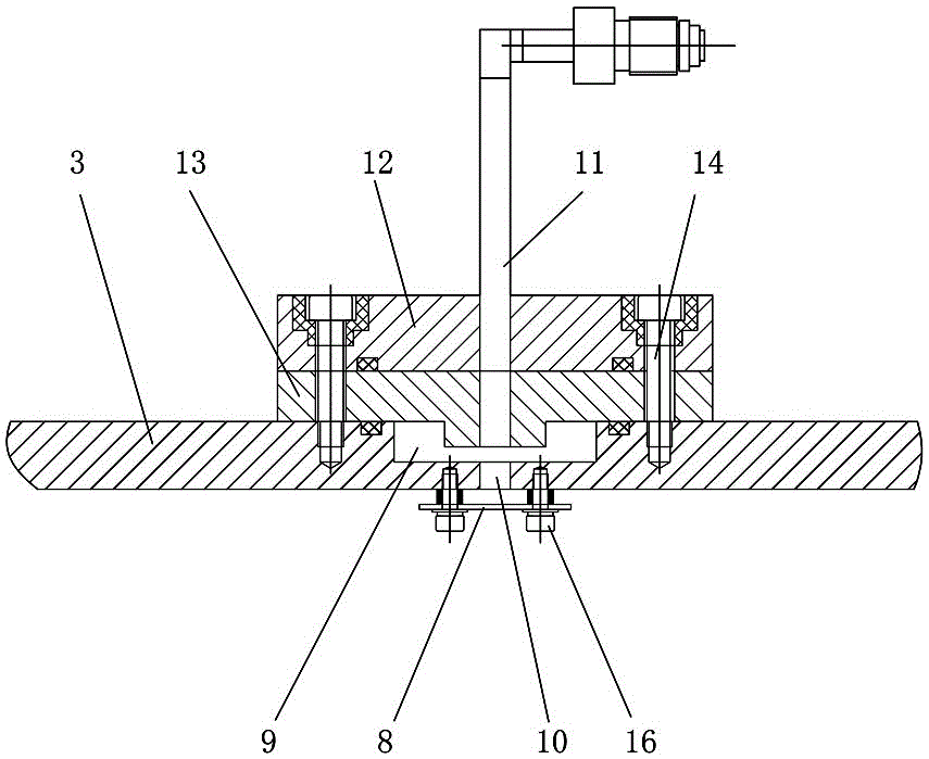
[0025] figure 1 and figure 2 An embodiment of the reaction chamber of the present invention is shown, which includes a closed chamber composed of a lower pad 3, a side wall 2 and an upper cover plate 1 and a flat heater assembly 4 disposed in the chamber A uniform flow plate 5 is provided between the upper cover plate 1 and the flat heater assembly 4, and a uniform flow chamber 6 is formed between the even flow plate 5 and the upper cover plate 1, and an air intake assembly 7 is provided on the upper cover plate 1 for further The air outlet of the gas assembly 7 communicates with the uniform flow chamber 6, and an air flow baffle 8 is arranged at a certain distance ahead of the air outlet of the air intake assembly 7, and the air flow baffle 8 is positioned directly in front of the air outlet of the air intake assembly 7 for blockin...


PUM


Abstract

The invention discloses a reaction cavity. The reaction cavity comprises a closed cavity body and a flat plate heater assembly, wherein the cavity body consists of a lower spacer, a side wall and an upper cover plate, the flat plate heater assembly is arranged in the cavity body, a flow equalizing plate is arranged between the upper cover plate and the flat plate heater assembly, a flow equalizing cavity is formed between the flow equalizing plate and the upper cover plate, an air inlet assembly is arranged on the upper cover plate, an air outlet of the air inlet assembly is communicated with the flow equalizing cavity, and an air flow baffle is arranged in a position which is of a certain distance from the air outlet of the air inlet assembly. The technical gas of the reaction cavity is equalized twice before entering the reaction cavity. The reaction cavity has the advantage that the technical gas enters at a high speed and is evenly distributed. The technical quality is improved, and the film forming quality of a semiconductor material is improved. As the technical gas directly enters the reaction cavity from the top of the cavity, the speed that the technical gas enters the reaction cavity is increased.

Description

technical field [0001] The invention relates to the technical field of semiconductor production, in particular to a reaction chamber and semiconductor processing equipment. Background technique [0002] Chemical vapor deposition is a gas phase growth method for preparing materials. It is to pass one or several compounds containing thin film elements and simple gas into the reaction chamber where the substrate is placed, and deposit on the surface of the substrate by means of space gas phase chemical reaction. Process technology for solid-state thin films. For the preparation of thin films on semiconductor wafers, the uniformity of thin films on the entire wafer surface is an extremely important indicator of the process, and closely related to this indicator is the distribution of electromagnetic fields, thermal fields, and airflow fields near the semiconductor wafer. Therefore, improving the distribution uniformity of the electromagnetic field, thermal field and airflow fie...

Claims


Application Information

Patent Timeline
Patent Type & Authority Applications(China)
IPC IPC(8): C23C16/455
Inventor 张宇田湘龙吴德轶胡昌文
Owner HUNAN RED SUN PHOTOELECTRICITY SCI & TECH
Why Eureka
Try Eureka