Circuit board with shielding structure and preparation method thereof

A shielding structure and circuit board technology, applied in the directions of printed circuit manufacturing, printed circuits, printed circuits, etc., can solve the problems affecting the performance of components on the circuit board, the warpage of the circuit board, etc., to improve the anti-interference function, the processing convenience, The effect of improving shielding performance

Active Publication Date: 2015-11-25
ZHEJIANG ZAPON ELECTRONICS TECH
View PDF6 Cites 0 Cited by
  • Summary
  • Abstract
  • Description
  • Claims
  • Application Information

AI Technical Summary

Problems solved by technology

[0003] The above technical solution solves the problem of warpage of the circuit board when passing through the reflow furnace, improves the production process to a certain extent, but

Method used


Image

  • Circuit board with shielding structure and preparation method thereof
  • Circuit board with shielding structure and preparation method thereof
  • Circuit board with shielding structure and preparation method thereof

Examples


Embodiment Construction

[0043] The following are specific embodiments of the present invention and in conjunction with the accompanying drawings, the technical solutions of the present invention are further described, but the present invention is not limited to these embodiments.

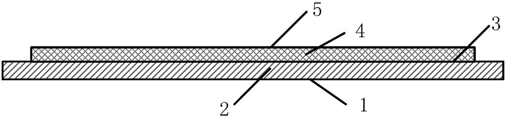
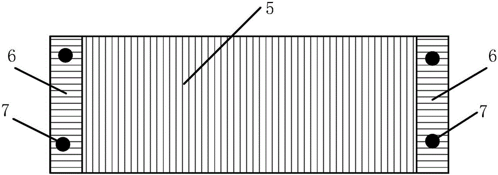
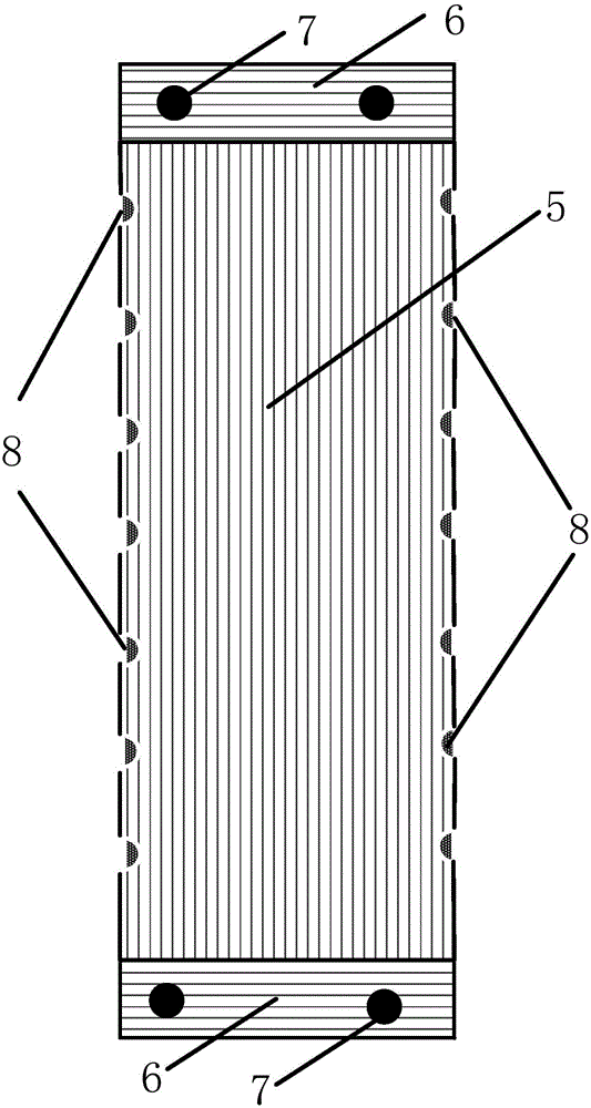
[0044] see figure 1 with figure 2 , is shown as a structural block diagram of a circuit board with a shielding structure provided by the present invention. A circuit board with a shielding structure includes a first shielding layer 1, a second shielding layer 5, and is arranged on the first shielding layer 1 and the shielding layer 5. The circuit layer 3 between the second shielding layer 5, the first insulating layer 2 arranged between the circuit layer 3 and the first shielding layer 1, the first insulating layer 2 arranged between the circuit layer 3 and the second shielding layer a second insulating layer 4 between shielding layers 5;

[0045] The second shielding layer 5 and the second insulating layer 4 are arrang...


PUM

PropertyMeasurementUnit
Diameteraaaaaaaaaa

Abstract

The present invention provides a circuit board with a shielding structure and a preparation method thereof. The circuit board includes: a first shielding layer, a second shielding layer, a circuit layer arranged between the first shielding layer and the second shielding layer, a first insulating layer arranged between the circuit layer and the first shielding layer, and a second insulating layer arranged between the circuit layer and the second shielding layer. The second shielding layer and the second insulating layer are arranged on the circuit layer and are smaller than the circuit layer in size. When the second shielding layer and the second insulating layer cover the circuit layer, at least one edge part of the circuit layer is exposed outside the second shielding layer, and the exposed edge part is provided with a plurality of metal electrodes connected to an external circuit board. According to the technical scheme of the present invention, shielding layers are arranged on two sides of the circuit layer so that a shielding processing to a circuit does not require a shielding cover; and the metal electrodes for connection on the circuit layer are exposed outside the insulating layer directly so as to avoid parasitic capacitances, and an anti-interference function of the circuit board is greatly enhanced.

Description

technical field [0001] The invention relates to the technical field of printed circuit boards, in particular to a circuit board with a shielding structure and a preparation method thereof. Background technique [0002] In some special application fields of circuit boards, such as remote sensing satellites, aerospace, radar communications, high-frequency antennas, microwave antennas and other applications, the stability and anti-interference requirements of circuit boards are extremely strict. In a complex environment, the circuit board must maintain stability; any weak interference signal may affect the normal operation of the circuit board, so the circuit board usually needs to be shielded. In the prior art, the metal shielding cover is usually welded on the circuit board to improve the anti-interference performance of the circuit board. The metal shielding cover needs to be welded at high temperature, which adds a process procedure, which not only increases the complexity ...

Claims


Application Information

Patent Timeline
IPC IPC(8): H05K1/02H05K3/00
CPCH05K1/0216H05K3/0011H05K2201/0707H05K2203/12
Inventor 黄骇
Owner ZHEJIANG ZAPON ELECTRONICS TECH
Why Eureka
Try Eureka