Liquid crystal panel and liquid crystal display device

A liquid crystal display device and liquid crystal panel technology, applied in the direction of instruments, nonlinear optics, optics, etc., can solve the problems of peripheral chromatic aberration, uneven thickness of the edge box of the liquid crystal panel, etc., and achieve the effect of eliminating peripheral chromatic aberration and uniform box thickness

Active Publication Date: 2018-09-18
KUSN INFOVISION OPTOELECTRONICS
View PDF8 Cites 0 Cited by
  • Summary
  • Abstract
  • Description
  • Claims
  • Application Information

AI Technical Summary

Problems solved by technology

When the motherboard of the liquid crystal panel is cut into a plurality of individual liquid crystal panels along the line A-A on the outside of the sealant 150, the edge of the liquid crystal panel will be subjected to additional force such as cutting stress, which will make the liquid crystal panel located on the edge of the liquid crystal panel The compression amount of the columnar spacers 140 at the edge is greater than the compression amount of the columnar spacers 140 in the middle of the liquid crystal panel, as figure 1 , after cutting, the edge will be lifted near the position of the sealant 150 in the figure, resulting in uneven cell thickness at the edge of the liquid crystal panel, and then peripheral chromatic aberration

Method used


Image

  • Liquid crystal panel and liquid crystal display device
  • Liquid crystal panel and liquid crystal display device
  • Liquid crystal panel and liquid crystal display device

Examples


Embodiment Construction

[0023] In order to further illustrate the technical means and functions adopted by the present invention to achieve the intended invention purpose, the present invention will be described in detail below in conjunction with the accompanying drawings and preferred embodiments.

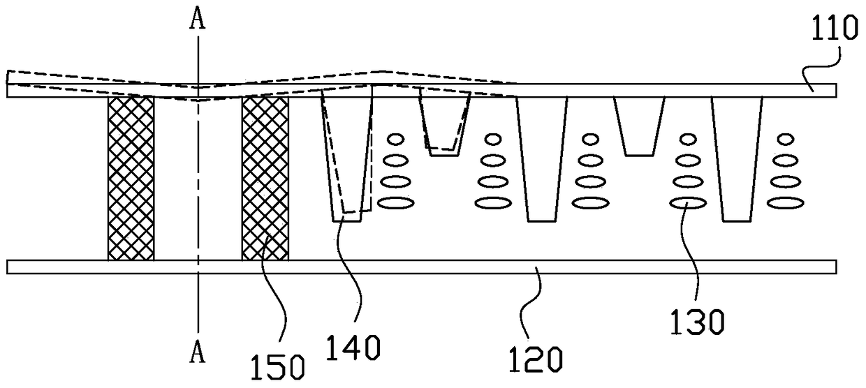
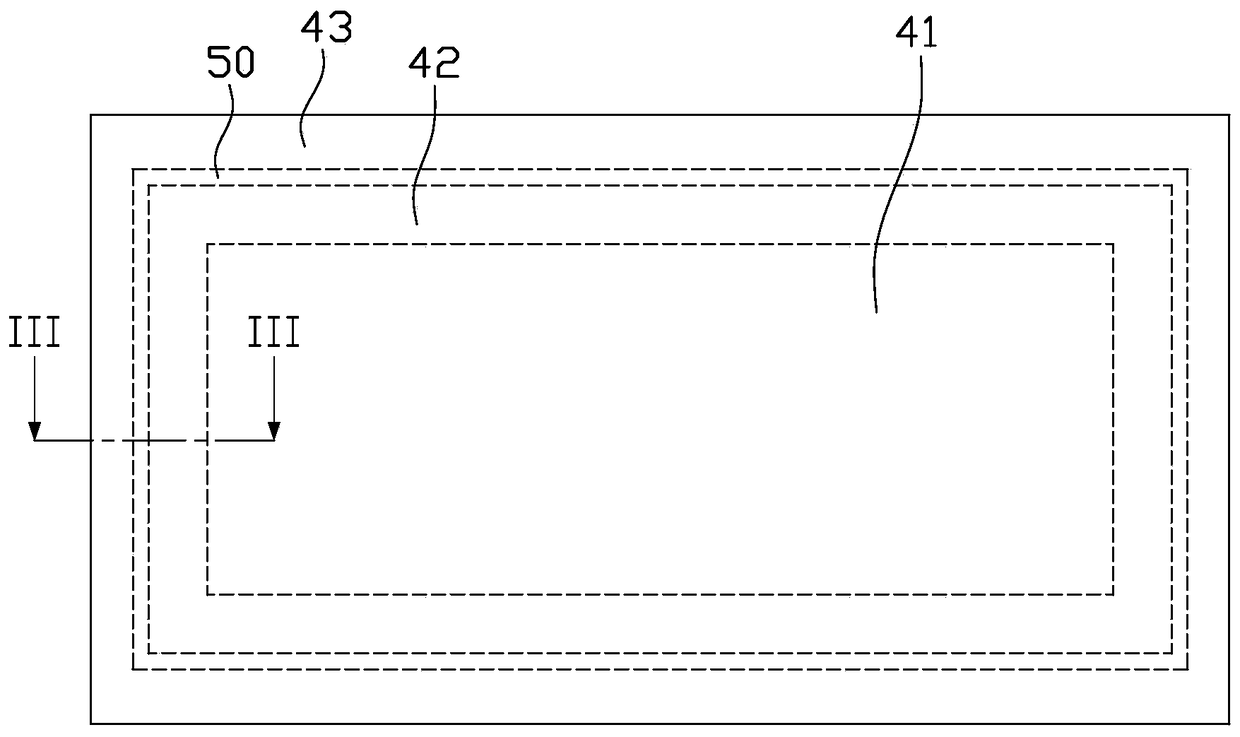
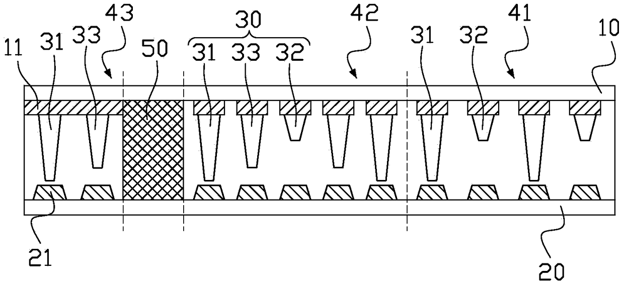
[0024] The invention provides a liquid crystal panel and a liquid crystal display device with the liquid crystal panel. figure 2 It is a schematic structural diagram of a liquid crystal panel in an embodiment of the present invention, image 3 for figure 2 Schematic diagram of the cross-sectional structure along the direction III-III, Figure 4 for image 3 The schematic diagram of the cross-sectional structure of the liquid crystal panel shown when it is compressed by force. Such as Figure 2 to Figure 4 As shown, the liquid crystal panel includes a CF (color filter) substrate 10, a TFT (Thin Film Transistor) substrate 20, a liquid crystal layer (not shown) filled between the CF substrate 10 and ...


PUM

PropertyMeasurementUnit
heightaaaaaaaaaa
heightaaaaaaaaaa
heightaaaaaaaaaa

Abstract

The invention provides a liquid crystal display panel which comprises a color filter substrate, an array substrate and a liquid crystal layer arranged between the color filter substrate and the array substrate in a filling mode. The liquid crystal display panel comprises an active area and a dummy area located between frame sealing glue and the active area. The active area and the dummy area between the color filter substrate and the array substrate are provided with main photo spacers and sub photo spacers. The height of the main photo spacers is larger than that of the sub photo spacers. The dummy area is further provided with transition photo spacers. The height of the transition photo spacers is lower than that of the main photo spacers but larger than that of the sub photo spacers. By means of the liquid crystal display panel and a liquid crystal display device, when the action force borne by the dummy area is larger than that of the active area, the transition photo spacers can offset the difference value between the action force borne by the dummy area and the action force borne by the active area through compression of the transition photo spacers, the cell thickness of the liquid crystal display panel is made to be even, and the peripheral color difference is eliminated.

Description

technical field [0001] The invention relates to the technical field of liquid crystal displays, in particular to a liquid crystal panel and a liquid crystal display device having the same. Background technique [0002] With the rapid development of electronic products towards lightness, thinness and miniaturization, almost all kinds of portable electronic products use liquid crystal displays (Liquid Crystal Display, LCD) as display terminals, especially in camcorders, notebook computers, desktops, etc. Computers, smart TVs, mobile terminals, personal digital processors and other products. [0003] However, in the prior art, chromatic aberration often occurs around the liquid crystal panel, that is, peripheral chromatic aberration, which in turn leads to poor quality of the display image of the liquid crystal display. This phenomenon is usually caused by uneven cell thickness (gap) at the edge of the liquid crystal panel due to limitations in design and manufacturing process...

Claims


Application Information

Patent Timeline
Patent Type & Authority Patents(China)
IPC IPC(8): G02F1/1339
CPCG02F1/13394G02F1/13396
Inventor 李沙
Owner KUSN INFOVISION OPTOELECTRONICS
Why Eureka
Try Eureka