Pnin/npip type utb-soi TFET with abrupt tunneling junction and preparation method
A UTB-SOITFET, UTB-SOI technology, applied in semiconductor/solid-state device manufacturing, electrical components, circuits, etc., can solve the problems of sub-threshold slope theoretical value degradation, small drive current, low leakage current, etc., to suppress bipolar effect, increase device drive current, and reduce process difficulty
- Summary
- Abstract
- Description
- Claims
- Application Information
AI Technical Summary
Problems solved by technology
Method used
Image

Examples
Embodiment 1
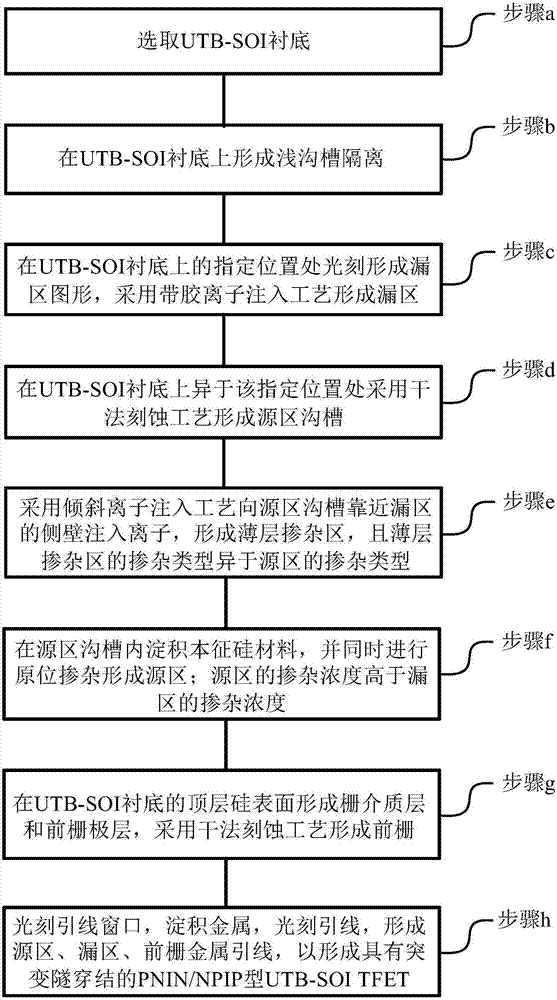
[0025] See figure 1 , figure 1 It is a flow chart of a preparation method of a PNIN / NPIP type UTB-SOITFET with a sudden tunnel junction according to an embodiment of the present invention, and the preparation method includes the following steps:
[0026] (a) Select Ultra-Thin-Body-Silicon-On-Insulator (UTB-SOI for short) substrate;
[0027] (b) Form shallow trench isolation on UTB-SOI substrate;
[0028] (c) Photolithographically form a drain region pattern at a specified position on the UTB-SOT substrate, and form a drain region by using an ion implantation process with glue;
[0029] (d) using a dry etching process to form a trench in the source region on the UTB-SOI substrate at a position other than the designated position;
[0030] (e) using an inclined ion implantation process to implant ions into the sidewall of the source trench near the drain region to form a thin-layer doped region, and the doping type of the thin-layer doped region is different from the doping ...
Embodiment 2
[0071] See Figure 2a-2i , Figure 2a-Figure 2i It is a schematic diagram of the preparation method of a PNIN / NPIP type UTB-SOI TFET with an abrupt tunneling junction according to an embodiment of the present invention, taking the preparation of a PNIN type UTB-SOI TFET with an abrupt tunneling junction with a channel length of 45 nm as an example for detailed description Instructions, the specific steps are as follows:
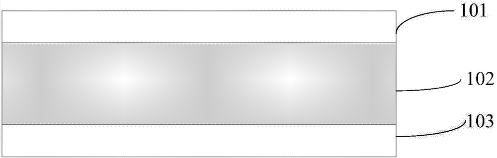
[0072] 1. Select UTB-SOI substrate
[0073] Such as Figure 2a , the crystal orientation of the UTB-SOI substrate 101 may be (100) or (110) or (111), without any limitation here, and the doping type of the UTB-SOI substrate 101 may be N type, It can also be P-type, with a doping concentration of 10 14 ~10 17 cm -3 , the thickness of the top layer Si is, for example, 10-20 nm.
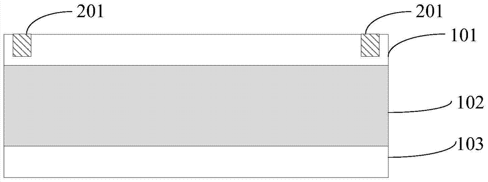
[0074] 2. Shallow trench isolation formation, such as Figure 2b shown.
[0075] 2.1 Form a first protective layer on the UTB-SOI substrate.
[0076] First, two layers of mat...
Embodiment 3
[0129] See image 3 , image 3 It is a structural schematic diagram of a PNIN / NPIP type UTB-SOITFET with an abrupt tunneling junction according to an embodiment of the present invention. The PNIN / NPIP UTB-SOITFET with an abrupt tunneling junction of the present invention includes an ultra-thin top silicon layer, a buried oxide Layer, underlying silicon layer, gate dielectric layer, front gate, back gate, highly doped source region, low doped drain region and N-type / P-type thin layer.
[0130] Specifically, the thickness of the ultra-thin fully depleted top silicon layer is preferably 10-20 nm, and the doping concentration is less than 10 17 cm -3 .
[0131] Specifically, the material of the gate dielectric layer can be selected from hafnium-based materials (a type of high dielectric constant material), such as HfO 2 , HfSiO, HfSiON, HfTaO, HfTiO or HfZrO or a combination thereof, other high dielectric constant materials such as Al 2 o 3 , La 2 o 3 , ZrO 2 Or one or a c...
PUM
 Abstract
Description
Claims
Application Information
 - R&D
- Intellectual Property
- Life Sciences
- Materials
- Tech Scout
- Unparalleled Data Quality
- Higher Quality Content
- 60% Fewer Hallucinations
Browse by: Latest US Patents, China's latest patents, Technical Efficacy Thesaurus, Application Domain, Technology Topic, Popular Technical Reports.
© 2025 PatSnap. All rights reserved.Legal|Privacy policy|Modern Slavery Act Transparency Statement|Sitemap|About US| Contact US: help@patsnap.com