Insulation layer upwards-expanded strained germanium tunneling field effect transistor (TFET) with abrupt tunneling junction and preparation method

A technology of straining germanium on an insulating layer, which is applied in semiconductor/solid-state device manufacturing, electrical components, diodes, etc., can solve the problems of subthreshold slope theoretical value degradation and small driving current, so as to suppress bipolar effect and improve mobility , Improve the effect of driving current and switching speed

Inactive Publication Date: 2016-01-06
XIAN UNIV OF SCI & TECH
View PDF2 Cites 0 Cited by
  • Summary
  • Abstract
  • Description
  • Claims
  • Application Information

AI Technical Summary

Problems solved by technology

[0005] In order to overcome the problems of low driving current of existing silicon-based TFET devices and the degradation of subthreshold slope relative to the theoretical value, the present invention proposes a tension-strained germanium TFET on an insulating layer with abrupt tunneling junction and its preparation method

Method used


Image

  • Insulation layer upwards-expanded strained germanium tunneling field effect transistor (TFET) with abrupt tunneling junction and preparation method
  • Insulation layer upwards-expanded strained germanium tunneling field effect transistor (TFET) with abrupt tunneling junction and preparation method
  • Insulation layer upwards-expanded strained germanium tunneling field effect transistor (TFET) with abrupt tunneling junction and preparation method

Examples


Embodiment 1

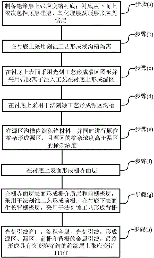
[0027] See figure 1 , figure 1 It is a flowchart of a method for preparing a tensile strained germanium TFET on an insulating layer with an abrupt tunnel junction according to an embodiment of the present invention, and the method includes the following steps:

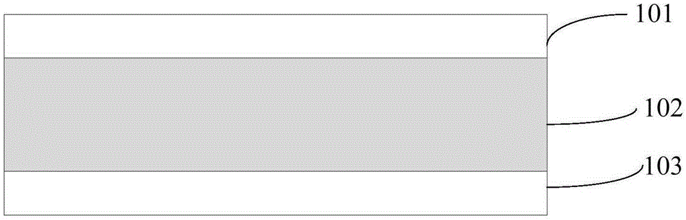
[0028] (a) preparing a tensile-strained germanium substrate on an insulating layer; the substrate sequentially includes a bottom silicon layer, a buried oxide layer and a top tensile-strained germanium layer from bottom to top;

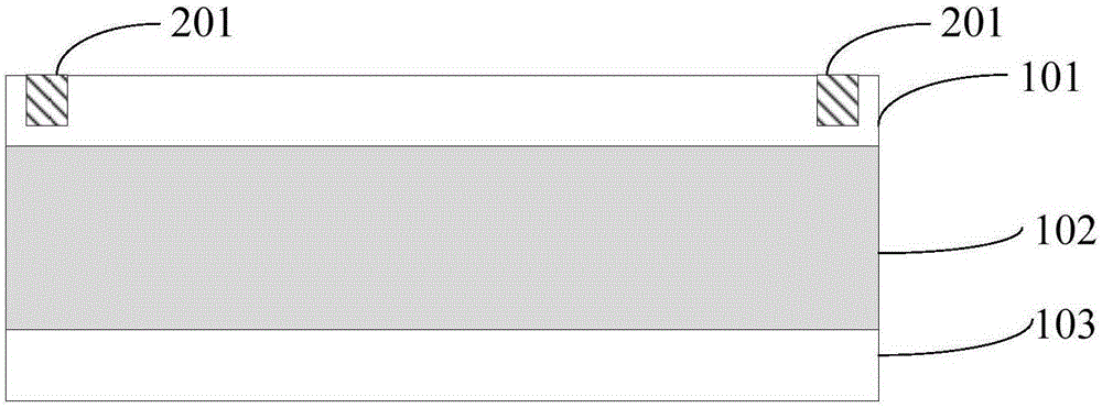
[0029] (b) forming shallow trench isolation on the substrate by an etching process;

[0030] (c) forming a drain region pattern on the upper surface of the substrate by a photolithography process and forming a drain region on the substrate by using an ion implantation process with glue;

[0031] (d) forming source region trenches on the substrate by a dry etching process;

[0032] (e) Depositing a germanium material in the trench of the source region, and simultaneously performing in-situ...

Embodiment 3

[0112] See image 3 , image 3 It is a schematic flow chart of a method for preparing a tensile-strained germanium-on-insulator TFET with an abrupt tunneling junction according to an embodiment of the present invention. To prepare an N-type tensile-strained germanium-on-insulator TFET with an abrupt tunneling junction with a channel length of 45 nm is An example is described in detail, and the specific steps are as follows:

[0113] 1. Preparation of strained germanium substrate on insulating layer

[0114] 1.1 Epitaxial growth.

[0115] Using molecular beam epitaxy (Molecular Beam Epitaxy, MBE) technology or metal organic chemical vapor deposition (MetalOrganic Chemical Vapour Deposition, MOCVD) technology, at the temperature of 400 ℃ to 450 ℃, epitaxial growth of 30nm to 120nm In composition graded In on the GaAs substrate x Ga 1-x As layer, where x is gradually changed from 0 to 0.3 or 0.35, and then a layer of In with fixed In composition is epitaxially grown at a temp...

Embodiment 4

[0175] See Figure 4 , Figure 4 It is a schematic diagram of the device structure of a tensile-strained germanium-on-insulator TFET with an abrupt tunneling junction according to an embodiment of the present invention. The tensile-strained germanium-on-insulator TFET with an abrupt tunneling junction of the present invention includes a fully depleted top-layer tensile-strained germanium layer, buried oxide layer, underlying silicon layer, high-K gate interface layer, high-K gate dielectric layer, front gate, back gate, highly doped source region and low doped drain region.

[0176] Specifically, the thickness of the fully depleted top tensile strained germanium layer can be selected from 20 to 30 nm, preferably 20 nm, and the doping concentration is less than 10 17 cm -3 .

[0177] Specifically, the gate interface layer is preferably yttrium oxide (Y 2 o 3 ) material, the high-K material layer can be selected from hafnium-based materials (a class of high dielectric constan...


PUM

PropertyMeasurementUnit
thicknessaaaaaaaaaa
thicknessaaaaaaaaaa
thicknessaaaaaaaaaa

Abstract

The invention relates to an insulation layer upwards-expanded strained germanium tunneling field effect transistor (TFET) with an abrupt tunneling junction and a preparation method. The preparation method comprises the following steps of: preparing an insulation layer upwards-expanded strained germanium substrate; forming shallow groove isolation by an etching process; forming a drain region pattern on the upper surface of the substrate by the etching process, and forming a drain region on the substrate by a glued ion implantation technology; forming a source region groove on the substrate by a dry etching process; depositing a germanium material in the source region groove, and simultaneously carrying out in-situ doping to form a source region; forming a grid interface layer, a grid dielectric layer and a front grid layer on the upper surface of the substrate, and forming a front grid by the dry etching process; growing a back grid layer on the lower surface of the substrate, and forming a back grid by the dry etching process; and carrying out photoetching of a lead window, metal deposition and lead photoetching, forming metal leads of the source region, the drain region, the front grid and the back grid, and finally forming the insulation layer upwards-expanded strained TFET with the abrupt tunneling junction.

Description

technical field [0001] The invention belongs to the technical field of semiconductor integrated circuits, and in particular relates to a tension-strained germanium TFET on an insulating layer with an abrupt tunnel junction and a preparation method thereof. Background technique [0002] Integrated Circuit (IC for short) technology follows the development of "Moore's Law" and has entered the nanoscale. Challenges from short channel effects, parasitic effects, and quantum tunneling make it increasingly difficult for traditional microelectronic device technology to meet the requirements of IC. The requirement of continuous technological development, especially the increasingly serious power consumption problem, has become the biggest bottleneck in continuing "Moore's Law". [0003] Tunneling Field Effect Transistor (Tunneling Field Effect Transistor, referred to as TFET) adopts the physical mechanism of band-band tunneling, so that its sub-threshold swing is not limited by the l...

Claims


Application Information

Patent Timeline
Patent Type & Authority Applications(China)
IPC IPC(8): H01L29/739H01L29/06H01L21/331
CPCH01L29/0603H01L29/66356H01L29/7391
Inventor 李妤晨张超张岩徐大庆秦学斌
Owner XIAN UNIV OF SCI & TECH
Why Eureka
Try Eureka