Pnin/npip type fd-goi TFET with abrupt tunneling junction and preparation method thereof

A tunneling junction and dry etching technology, which is applied in the manufacture of semiconductor/solid-state devices, electrical components, circuits, etc., can solve the problems of small driving current, reduced sub-threshold slope, and degradation of the theoretical value of sub-threshold slope. Bipolar effect, the effect of reducing the difficulty of the process

Inactive Publication Date: 2017-11-03
XIAN UNIV OF SCI & TECH
View PDF3 Cites 0 Cited by
  • Summary
  • Abstract
  • Description
  • Claims
  • Application Information

AI Technical Summary

Problems solved by technology

[0004] In order to overcome the problems of low driving current of existing silicon-based TFET devices and the degradation of subthreshold slope relative to the theoretical value, the present invention proposes a PNIN / NPIP type FD-GOI TFET with abrupt tunneling junction and its preparation method, which can effectively improve the TFET device drive current as well as reducing the subthreshold slope

Method used


Image

  • Pnin/npip type fd-goi TFET with abrupt tunneling junction and preparation method thereof
  • Pnin/npip type fd-goi TFET with abrupt tunneling junction and preparation method thereof
  • Pnin/npip type fd-goi TFET with abrupt tunneling junction and preparation method thereof

Examples


Embodiment 1

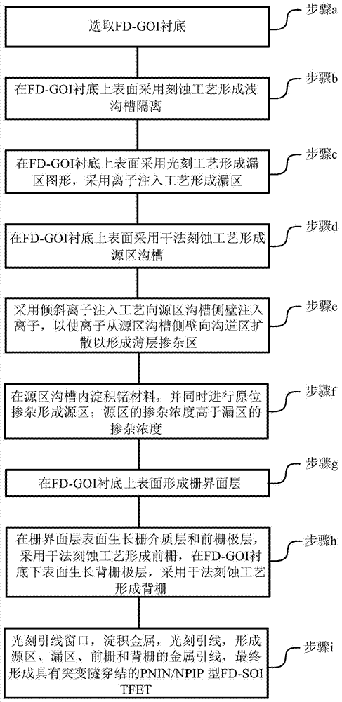
[0026] See figure 1 , figure 1 It is a flow chart of a preparation method of a PNIN / NPIP type FD-GOITFET with a sudden tunnel junction according to an embodiment of the present invention, and the preparation method includes the following steps:

[0027] (a) Select a fully depleted germanium-on-insulator (Fully Depleted Germanium-On-Insulator, referred to as FD-GOI) substrate;

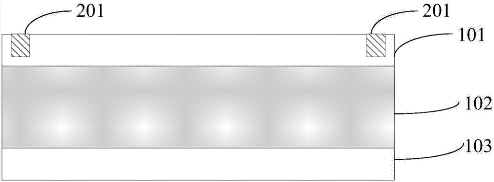
[0028] (b) Form shallow trench isolation on the upper surface of the FD-GOI substrate by etching;

[0029] (c) forming a drain region pattern on the upper surface of the FD-GOI substrate by photolithography, and forming a drain region by ion implantation;

[0030] (d) forming a source region trench on the upper surface of the FD-GOI substrate by a dry etching process;

[0031] (e) implanting ions into the sidewall of the trench in the source region by using an inclined ion implantation process, so that the ions diffuse from the sidewall of the trench in the source region to the channel region to fo...

Embodiment 2

[0076] See Figure 2a-2i , Figure 2a-Figure 2i It is a schematic diagram of the preparation method of a PNIN / NPIP type FD-GOI TFET with an abrupt tunneling junction according to an embodiment of the present invention, taking the preparation of a PNIN type FD-GOI TFET with an abrupt tunneling junction with a channel length of 45 nm as an example for detailed description. Instructions, the specific steps are as follows:

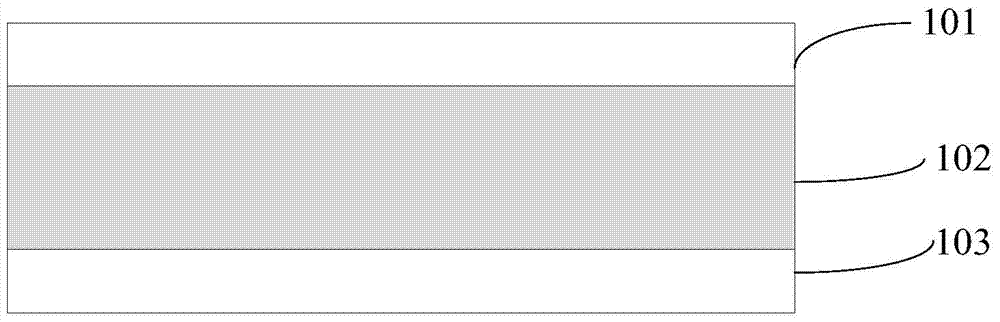
[0077] 1. Select the FD-GOI substrate.

[0078] Such as Figure 2a , the FD-GOI substrate includes a top layer of germanium 101, an oxide buried layer 102 such as a silicon dioxide layer buried layer, and a bottom layer of silicon 103, and the crystal orientation of the FD-GOI substrate 101 can be (100) or (110) or ( 111), without any limitation here, in addition, the doping type of the FD-GOI substrate 101 can be N-type or P-type, and the doping concentration is, for example, 10 14 ~10 17 cm -3 The thickness of the top layer Si is, for example, 20-100 n...

Embodiment 3

[0135] See image 3 , image 3 It is a schematic structural diagram of a PNIN / NPIP type FD-GOITFET with an abrupt tunneling junction according to an embodiment of the present invention. The PNIN / NPIP FD-GOITFET with an abrupt tunneling junction of the present invention includes a fully depleted top germanium layer, a buried Oxygen layer, underlying silicon layer, gate interface layer, gate dielectric layer, front gate, back gate, heavily doped source region, low doped drain region and N-type / P-type thin layer.

[0136] Specifically, the thickness of the fully depleted top germanium layer can be selected from 20 to 100 nm, preferably 20 nm, and the doping concentration is less than 10 17 cm -3 .

[0137] Specifically, the gate interface layer is preferably yttrium oxide (Y 2 o 3 ) material, the high-K material layer can be selected from hafnium-based materials (a class of high dielectric constant materials), such as HfO 2 , HfSiO, HfSiON, HfTaO, HfTiO or HfZrO or a combinat...


PUM


Abstract

The invention relates to a PNIN / NPIP type fully-depleted-silicon-on-insulator (FD-GOI) TFET with an abrupt tunnel junction and a preparation method thereof. The preparation method comprises: an FD-GOI substrate is selected; an etching process is carried out to form a shallow-trench isolation unit; a photoetching process is carried out form a drain region graph and an ion implantation technology is used for forming a drain region; a source region trench is formed in the upper surface of the substrate; ion implantation is carried out on the side wall of the source region trench by using an angled ion implantation technology to form a thin-layer doping region; germanium material deposition is carried out on the source region trench and in-situ doping is carried out simultaneously to form a source region; the doping concentration of the source region is higher than that of the drain region; a gate interface layer is formed on the upper surface of the substrate; a gate dielectric layer and a front gate layer grow on the surface of the gate interface layer and a dry etching process is used for forming a front gate, a back gate layer grows on the lower surface of the substrate, and a dry etching process is used for forming a back gate; lead window photoetching, metal deposition, and lead photoetching are carried out to form metal leads of the source region, the drain region, the front gate, and the back gate, thereby forming the PNIN / NPIP type FD-GOI TFET with an abrupt tunnel junction.

Description

technical field [0001] The invention belongs to the technical field of semiconductor integrated circuits, and in particular relates to a PNIN / NPIP type FD-GOI TFET with an abrupt tunnel junction and a preparation method. Background technique [0002] The development of Integrated Circuit (IC) technology follows the "Moore's Law" and has entered the nanometer scale. Challenges from short channel effects, parasitic effects, and quantum tunneling make it increasingly difficult for traditional microelectronic device technology to meet The requirements for the continuous development of IC technology, especially the increasingly serious power consumption problem, have become the biggest bottleneck in the continuation of "Moore's Law". [0003] The tunneling field effect transistor (Tunneling Field Effect Transistor, referred to as TFET) adopts the physical mechanism of band-band tunneling, so that its sub-threshold swing breaks through the limitation of the traditional MOSFET sub-...

Claims


Application Information

Patent Timeline
Patent Type & Authority Patents(China)
IPC IPC(8): H01L21/336H01L21/265H01L21/762H01L21/28H01L29/78H01L29/06H01L29/08H01L29/423
CPCH01L21/26506H01L21/7624H01L29/0688H01L29/0847H01L29/401H01L29/4232H01L29/66484H01L29/7831
Inventor 李妤晨
Owner XIAN UNIV OF SCI & TECH
Why Eureka
Try Eureka