PNIN/NPIP type tensile strained germanium on insulator TFET with abrupt tunneling junctions and preparation method thereof

A technology of straining germanium on an insulating layer, applied in semiconductor/solid-state device manufacturing, semiconductor devices, electrical components, etc. Pole effect, increased mobility, and reduced process difficulty

Inactive Publication Date: 2016-01-13
XIAN UNIV OF SCI & TECH
View PDF3 Cites 0 Cited by
  • Summary
  • Abstract
  • Description
  • Claims
  • Application Information

AI Technical Summary

Problems solved by technology

[0004] In order to overcome the problems of low driving current of the existing silicon-based TFET devices and the degradation of the subthreshold slope relative to the theoretical value, the present invention proposes a PNIN / NPIP type insulating layer tension-strained germanium TFET with abrupt tunneling junctions and a preparation method thereof, which can be used Effectively increase the driving current of TFET devices and reduce the subthreshold slope

Method used


Image

  • PNIN/NPIP type tensile strained germanium on insulator TFET with abrupt tunneling junctions and preparation method thereof
  • PNIN/NPIP type tensile strained germanium on insulator TFET with abrupt tunneling junctions and preparation method thereof
  • PNIN/NPIP type tensile strained germanium on insulator TFET with abrupt tunneling junctions and preparation method thereof

Examples


Embodiment 1

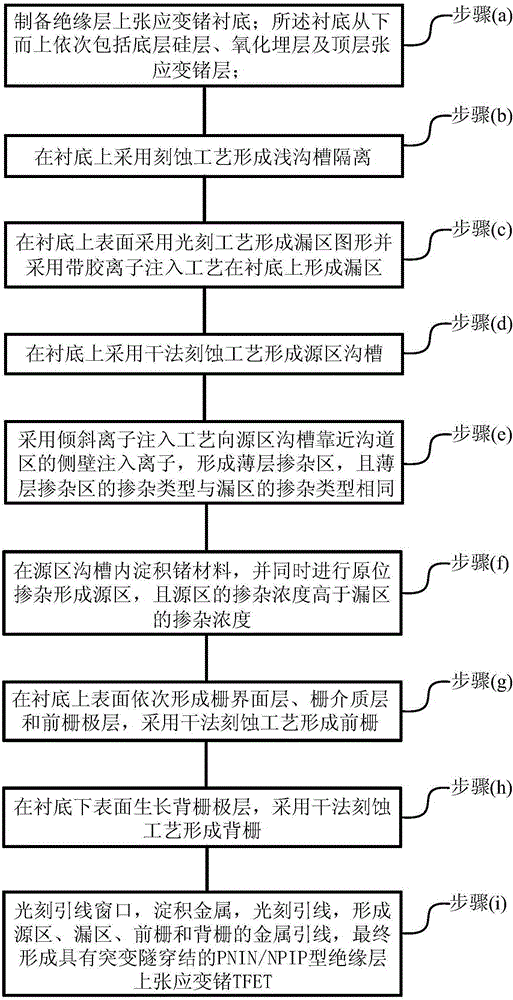
[0026] See figure 1 , figure 1 A method for preparing a tensile strained germanium TFET on a PNIN / NPIP type insulating layer with an abrupt tunnel junction according to an embodiment of the present invention picture , the preparation method comprises the steps of:

[0027] (a) preparing a tensile-strained germanium substrate on an insulating layer; the substrate sequentially includes a bottom silicon layer, a buried oxide layer and a top tensile-strained germanium layer from bottom to top;

[0028] (b) forming shallow trench isolation on the substrate by an etching process;

[0029] (c) forming a drain region pattern on the upper surface of the substrate by a photolithography process and forming a drain region on the substrate by using an ion implantation process with glue;

[0030] (d) forming source region trenches on the substrate by a dry etching process;

[0031] (e) using an inclined ion implantation process to implant ions into the sidewall of the source tren...

Embodiment 2

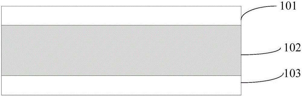
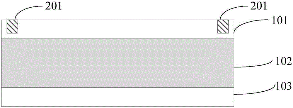
[0078] See Figure 2a -2i, Figure 2a - Figure 2i Schematic illustration of a method for preparing a PNIN / NPIP-type insulating layer-on-tensile germanium TFET with an abrupt tunneling junction according to an embodiment of the present invention picture , taking the preparation of a PNIN-type tensile strained germanium-on-insulator TFET with a channel length of 45 nm and an abrupt tunneling junction as an example to describe in detail, the specific steps are as follows:

[0079] 1. Prepare a strained germanium substrate on an insulating layer. Such as Figure 2a , the tensile-strained germanium-on-insulator substrate includes a top layer of tensile-strained germanium 101 , a buried oxide layer 102 such as a buried layer of silicon dioxide, and a bottom layer of silicon 103 .

[0080] 1.1 Epitaxial growth.

[0081] Using molecular beam epitaxy (Molecular Beam Epitaxy, MBE) technology or metal organic chemical vapor deposition (MetalOrganic Chemical Vapour Depositio...

Embodiment 3

[0143] See image 3 , image 3 Schematic diagram of the structure of a PNIN / NPIP-type insulator-on-insulator tension-strained germanium TFET with an abrupt tunnel junction according to an embodiment of the present invention picture The tensile strained germanium TFET on the PNIN / NPIP insulating layer with abrupt tunneling junction of the present invention comprises a fully depleted top tensile strained germanium layer, a buried oxide layer, a bottom silicon layer, a gate interface layer, a gate dielectric layer, a front gate, a back gate Gate, heavily doped source region, low doped drain region and N-type / P-type thin layer.

[0144] Specifically, the thickness of the fully depleted top tensile strained germanium layer can be selected from 20 to 30 nm, preferably 20 nm, and the doping concentration is less than 10 17 cm -3 .

[0145] Specifically, the gate interface layer is preferably yttrium oxide (Y 2 o 3 ) material, the high-K material layer can be selected from ha...


PUM

PropertyMeasurementUnit
thicknessaaaaaaaaaa
thicknessaaaaaaaaaa
thicknessaaaaaaaaaa

Abstract

The invention relates to a PNIN / NPIP type tensile strained germanium on insulator TFET with abrupt tunneling junctions and a preparation method thereof. The preparation method comprises the steps that a tensile strained germanium on insulator substrate is prepared; shallow trench isolation is formed by adopting an etching technology; a drain region pattern is formed on the upper surface of the substrate by adopting a photoetching technology and a drain region is formed by adopting an adhesive ion injection technology; a source region trench is formed on the substrate by adopting the etching technology; ions are injected in the side wall of the source region trench close to a channel region by adopting an inclined ion injection technology so that a thin layer doped region is formed; germanium material is deposited in the source region trench and in-situ doping is performed so that a source region is formed; a gate interface layer, a gate dielectric layer and a front gate layer are formed on the upper surface of the substrate in turn, and a front gate is formed by adopting the etching technology; a back gate layer is grown on the lower surface of the substrate, and a back gate is formed by adopting the etching technology; and a lead-wire window is photoetched, metal is deposited and a lead-wire is photoetched so that a metal lead-wire of the source region, the drain region, the front gate and the back gate is formed, and finally the PNIN / NPIP type tensile strained germanium on insulator TFET with the abrupt tunneling junctions is formed.

Description

technical field [0001] The invention belongs to the technical field of semiconductor integrated circuits, and in particular relates to a tension-strained germanium TFET on a PNIN / NPIP type insulating layer with an abrupt tunnel junction and a preparation method. Background technique [0002] Integrated Circuit (IC for short) technology follows the development of "Moore's Law" and has entered the nanoscale. Challenges from short channel effects, parasitic effects, and quantum tunneling make it increasingly difficult for traditional microelectronic device technology to meet the requirements of IC. The requirement of continuous technological development, especially the increasingly serious power consumption problem, has become the biggest bottleneck in continuing "Moore's Law". [0003] Tunneling Field Effect Transistor (Tunneling Field Effect Transistor, referred to as TFET) adopts the physical mechanism of band-band tunneling, so that its sub-threshold swing breaks through th...

Claims


Application Information

Patent Timeline
Patent Type & Authority Applications(China)
IPC IPC(8): H01L21/335H01L29/772H01L21/265H01L29/08H01L21/762
CPCH01L21/265H01L21/7624H01L29/08H01L29/0843H01L29/66409H01L29/772
Inventor 李妤晨徐大庆秦学斌
Owner XIAN UNIV OF SCI & TECH
Why Eureka
Try Eureka