Pnin/npip type ssoi TFET with abrupt tunneling junction and preparation method thereof

A technology of tunneling junction and dry etching, which is applied in semiconductor/solid-state device manufacturing, electrical components, diodes, etc., can solve the problems of limiting the tunneling probability of TFET devices, reducing the average sub-threshold slope, and small driving current, etc., to achieve Effects of suppressing bipolar effects, increasing the probability of tunneling, and reducing the forbidden band width

Inactive Publication Date: 2018-01-05
XIAN UNIV OF SCI & TECH
View PDF3 Cites 0 Cited by
  • Summary
  • Abstract
  • Description
  • Claims
  • Application Information

AI Technical Summary

Problems solved by technology

However, there are not many experimental reports of traditional Si-based TFET devices breaking through 60 mV / dec, and the subthreshold slope of TFET devices is still a function of gate voltage, and its value tends to deteriorate with the increase of gate voltage. The average subthreshold slope of the device is a difficult problem
In addition, Si material is an indirect bandgap semiconductor, and the bandgap width is relatively large, which limits the tunneling probability of TFET devices. Therefore, compared with traditional MOSFET devices, the driving current of this device is smaller

Method used


Image

  • Pnin/npip type ssoi TFET with abrupt tunneling junction and preparation method thereof
  • Pnin/npip type ssoi TFET with abrupt tunneling junction and preparation method thereof
  • Pnin/npip type ssoi TFET with abrupt tunneling junction and preparation method thereof

Examples


Embodiment 1

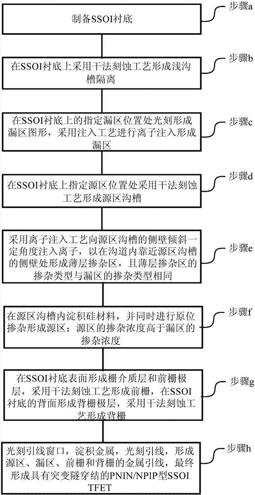
[0026] See figure 1 , figure 1 It is a flow chart of a preparation method of a PNIN / NPIP type SSOI TFET with an abrupt tunneling junction according to an embodiment of the present invention. The preparation method includes the following steps:

[0027] (a) Preparation of SSOI substrate;

[0028] (b) Using a dry etching process to form shallow trench isolation on the SSOI substrate;

[0029] (c) Forming a drain region pattern by photolithography at a designated drain region position on the SSOI substrate, and performing ion implantation using an implantation process to form the drain region;

[0030] (d) Using a dry etching process to form a source region trench at a designated source region location on the SSOI substrate;

[0031] (e) Using an ion implantation process to implant ions at an oblique angle to the sidewall of the source region trench to form a thin doped region in the trench near the sidewall of the source region trench, and the thin layer The doping type of the doped re...

Embodiment 2

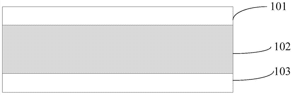
[0076] See Figure 2a-2i , Figure 2a-Figure 2i It is a schematic diagram of the preparation method of a PNIN / NPIP type SSOI TFET with abrupt tunneling junction according to an embodiment of the present invention, taking the preparation of a PNIN type SSOITFET with a sudden tunneling junction with a channel length of 45nm as an example for detailed description. The specific steps are as follows :

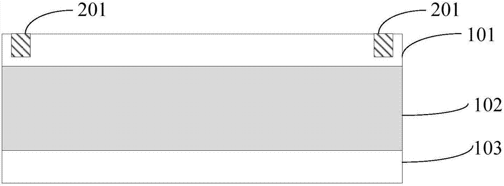
[0077] 1. Prepare SSOI substrate, such as Figure 2a Shown:

[0078] 1.1 Epitaxial growth.

[0079] Using selective epitaxy technology, a graded SiGe layer is epitaxially grown on a Si wafer at a high temperature of 800°C to 900°C, by dynamically adjusting the gas phase precursor GeH during the epitaxial growth process 4 And SiH 2 Cl 2 To control the Ge composition of the graded SiGe layer to increase the Ge composition of the relaxed SiGe layer from 0 to a fixed composition, and then epitaxially grow a fixed composition at a high temperature of 800°C to 900°C Relaxed Si 1-x Ge x Layer, w...

Embodiment 3

[0140] See image 3 , image 3 It is a schematic structural diagram of a PNIN / NPIP type SSOITFET with abrupt tunneling junction according to an embodiment of the present invention. The PNIN / NPIP SSOI TFET with abrupt tunneling junction of the present invention includes a top strained Si layer, a buried oxide layer, and a bottom Si layer , Gate dielectric layer, front gate, back gate, highly doped source region, low doped drain region and N-type / P-type thin layer.

[0141] Specifically, the SSOI substrate is prepared by smart stripping technology, the Ge component of the strain-inducing layer SiGe layer is preferably 0.4, the strained Si layer is directly on the insulating layer, and there is no strain-inducing layer SiGe layer under it, and the thickness of the strained Si layer is preferably 10-20nm, the thickness is less than the critical thickness of strained Si when the Ge composition is 0.4, and the doping concentration is less than 10 17 cm -3 .

[0142] Specifically, the gate ...


PUM


Abstract

The invention relates to a PNIN / NPIP type SSOI TFET with abrupt tunneling junctions and a preparation method thereof. The preparation method comprises the steps that an SSOI substrate is prepared; shallow trench isolation is formed; a drain region pattern is formed through photoetching, and adhesive ions are injected so that a drain region is formed; a source region trench is formed through dry etching; the ions are injected in the side wall of the source region trench at a certain inclined angle by adopting an ion injection technology, Si material is deposited in the source region trench, and in-situ doping is performed so that a source region is formed; a gate dielectric layer and a front gate layer are formed on the upper surface of the substrate, a front gate is formed through etching, a back gate layer is formed on the lower surface of the substrate, and a back gate is formed through etching; and a lead-wire window is photoetched, metal is deposited and a lead-wire is photoetched so that source / drain and front / back gate lead-wires are formed. Drive current of the TFET can be effectively enhanced and subthreshold slope of the TFET can be reduced.

Description

Technical field [0001] The invention belongs to the technical field of semiconductor integrated circuits, and particularly relates to a PNIN / NPIP type SSOI TFET with an abrupt tunneling junction and a preparation method. Background technique [0002] The development of Integrated Circuit (IC) technology follows the "Moore's Law" and has entered the nanoscale. Challenges from short-channel effects, parasitic effects, and quantum tunneling have made traditional microelectronic device technologies increasingly difficult to meet The continuous development of IC technology, especially the increasingly serious power consumption problem, has become the biggest bottleneck for the continuation of "Moore's Law". [0003] Tunneling Field Effect Transistor (TFET) uses a band-band tunneling physical mechanism to make its sub-threshold swing not restricted by the traditional MOSFET sub-threshold swing limit KT / q, and has a small off-state current , The advantages of good frequency characteristi...

Claims


Application Information

Patent Timeline
Patent Type & Authority Patents(China)
IPC IPC(8): H01L29/66H01L21/762H01L29/739
CPCH01L21/76254H01L29/66356H01L29/7391
Inventor 李妤晨
Owner XIAN UNIV OF SCI & TECH
Why Eureka
Try Eureka