Thin film transistor, goa gate drive circuit, array substrate and display device

A technology of gate drive circuit and thin film transistor, which is applied in the field of GOA gate drive circuit, array substrate and display device, and thin film transistor, and can solve problems such as short circuit and uneven etching

Active Publication Date: 2018-03-27
BOE TECH GRP CO LTD +1
View PDF4 Cites 0 Cited by
  • Summary
  • Abstract
  • Description
  • Claims
  • Application Information

AI Technical Summary

Problems solved by technology

[0005] The purpose of the present invention is to provide a thin film transistor, a GOA gate drive circuit, an array substrate and a display device to solve the problem of short circuit between source and drain caused by uneven etching

Method used


Image

  • Thin film transistor, goa gate drive circuit, array substrate and display device
  • Thin film transistor, goa gate drive circuit, array substrate and display device
  • Thin film transistor, goa gate drive circuit, array substrate and display device

Examples


Embodiment 1

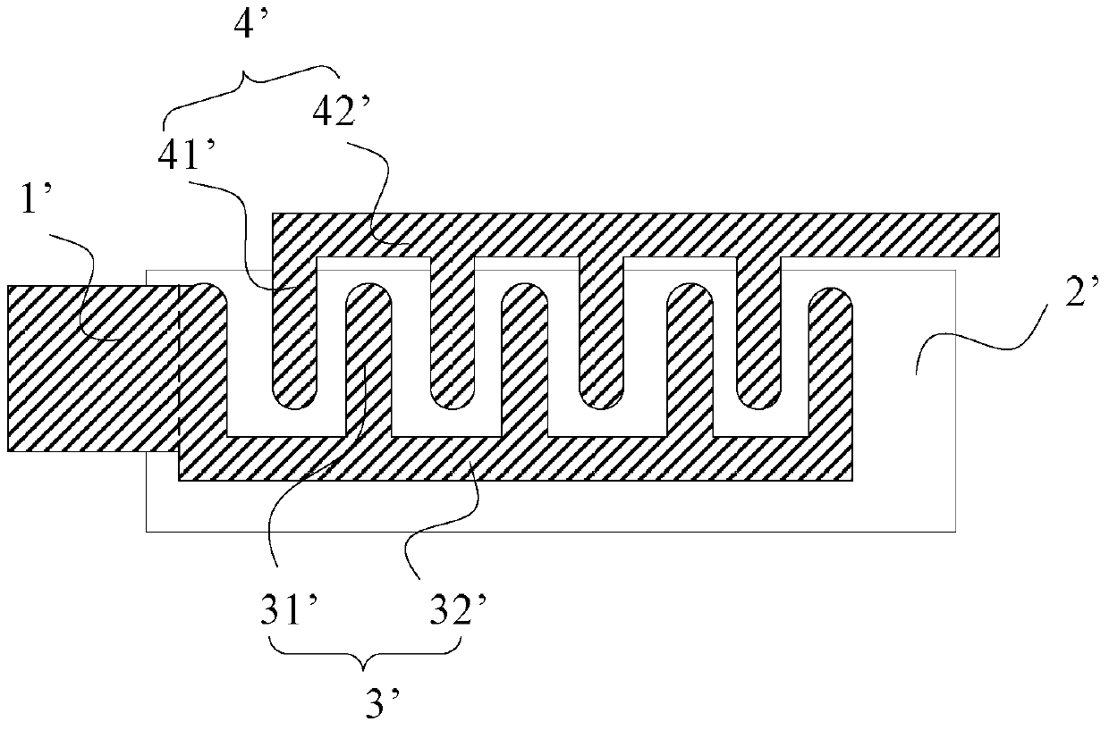
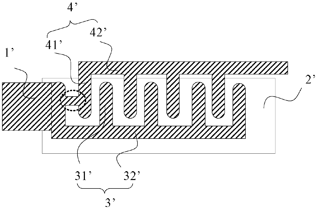
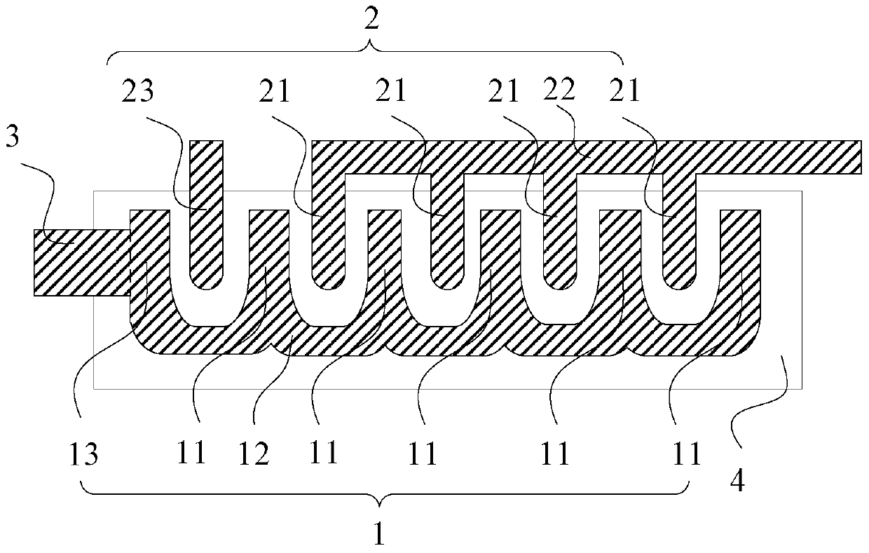
[0030] An embodiment of the present invention provides a thin film transistor, such as image 3 As shown, the thin film transistor includes comb-shaped source 1 and drain 2 arranged in the same layer, the source 1 is connected to the source lead 3, and the source 1 includes a plurality of first source comb teeth 11 and connected Source comb handles 12 of a plurality of first source comb teeth 11, the drain 2 includes at least one first drain comb teeth 21 and a drain comb handle 22 connected to the first drain comb teeth 21, The first source comb-tooth portion 11 and the first drain electrode comb-tooth portion 21 are arranged at intervals, and the source 1 further includes a second source electrode comb-tooth portion 13 which is connected to the source comb-tooth portion 12 , and connected to the source lead 3; the drain 2 also includes a second drain comb located between the second source comb-tooth portion 13 and the first source comb-tooth portion 11 adjacent to the second...


PUM


Abstract

The invention discloses a thin-film transistor, a gate driver on array (GOA) gate drive circuit, an array substrate and a display device, and relates to the technical field of display. The problem of a short circuit, caused by uneven etching, between a source electrode and a drain electrode can be solved. The thin-film transistor comprises a source electrode and the drain electrode, which are arranged at the same layer and are in a comb form respectively; the source electrode is connected with a source electrode lead; the source electrode comprises a plurality of first source electrode comb tooth parts, a source electrode comb handle part and a second source electrode comb tooth part; the source electrode comb handle part is connected with the plurality of first source electrode comb tooth parts; the drain electrode comprises at least one first drain electrode comb tooth part, a drain electrode comb handle part and a second drain electrode comb tooth part; the drain electrode comb handle part is connected with the first drain electrode comb tooth part; the second source electrode comb tooth part is connected with the source electrode comb handle part and is connected with the source electrode lead; the second drain electrode comb tooth part is located between the second source electrode comb tooth part and the first source electrode comb tooth part close to the second source electrode comb tooth part; and the second drain electrode comb tooth part is not connected with the drain electrode comb handle part. The thin-film transistor disclosed by the invention can be applied to the array substrate.

Description

technical field [0001] The invention relates to the field of display technology, in particular to a thin film transistor, a GOA gate drive circuit, an array substrate and a display device. Background technique [0002] Gate Driver on Array (GOA for short) technology is one of the gate drive technologies for display devices. The basic concept of GOA technology is to integrate the GOA gate drive circuit of the display device on the array substrate without external GOA. The gate driving circuit can reduce the frame of the display device. [0003] In the prior art, an array substrate using GOA technology includes a GOA gate drive circuit, such as figure 1 As shown, the GOA gate drive circuit includes a thin film transistor and a source lead 1', wherein the thin film transistor includes comb-shaped source 3' and drain 4' respectively arranged in the same layer, and a gate 2'; the source The pole 3' includes a plurality of comb teeth 31' and a comb handle 32' connected to the pl...

Claims


Application Information

Patent Timeline
Patent Type & Authority Patents(China)
IPC IPC(8): H01L29/786H01L29/417H01L27/12G02F1/1362
CPCG02F1/1362H01L27/1214H01L29/41733H01L29/786
Inventor 王宝强朴相镇
Owner BOE TECH GRP CO LTD
Why Eureka
Try Eureka