High speed PCB laminating method

A high-speed, steel plate technology, applied in chemical instruments and methods, lamination, lamination devices, etc., can solve problems such as reliability risks, and achieve good manufacturability, strong practicability, and easy promotion.

Inactive Publication Date: 2015-12-09
LANGCHAO ELECTRONIC INFORMATION IND CO LTD
View PDF5 Cites 9 Cited by
  • Summary
  • Abstract
  • Description
  • Claims
  • Application Information

AI Technical Summary

Problems solved by technology

Resin bleeding from this prepreg poses a serious reliability risk to the PCB
In addition, in the process of high-speed PCB production, because the customer requires that the thickness of the insulating layer of the PCB be increased from ±10% to within ±5%, due to resin outflow, the edge part is thinner than the middle part. This difference is currently about 7%. can no longer meet the demand

Method used


Image

  • High speed PCB laminating method
  • High speed PCB laminating method
  • High speed PCB laminating method

Examples


Embodiment Construction

[0022] The present invention will be further described below in conjunction with the accompanying drawings and specific embodiments.

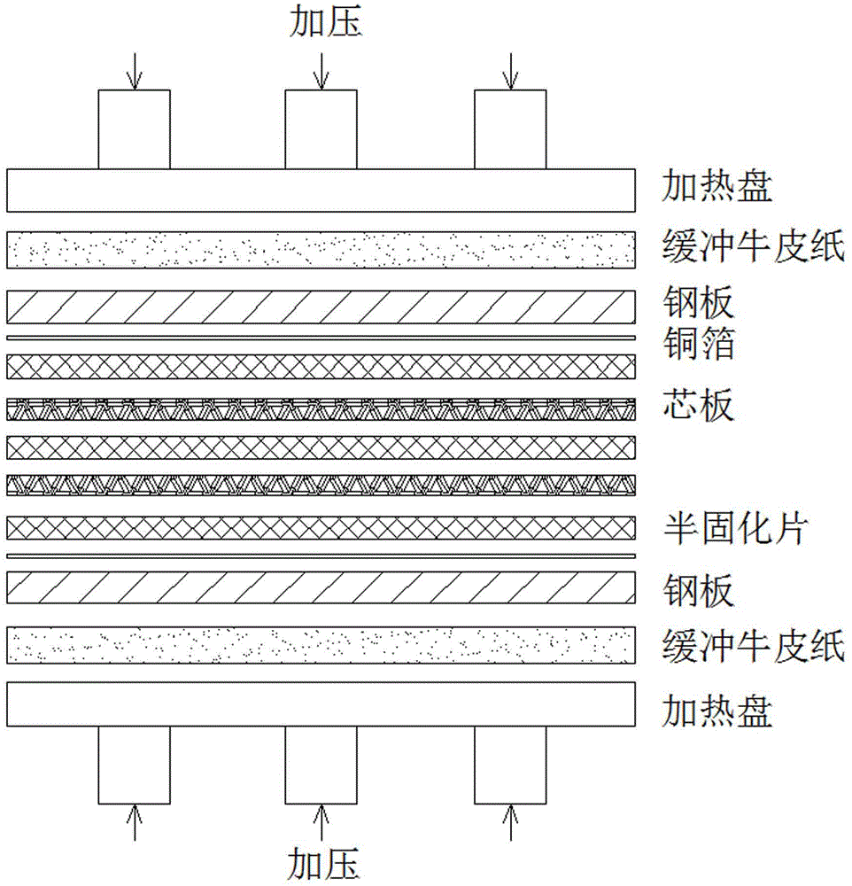
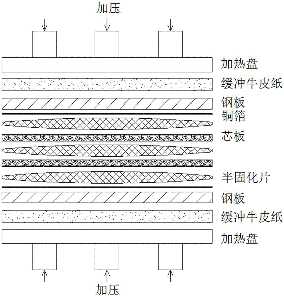
[0023] The invention provides a high-speed PCB lamination method, and proposes a scheme to optimize the internal stress mode of the PCB and pre-compensate the edge part of the PCB. The layers include a copper foil layer, several core board layers, and a copper foil layer from top to bottom, and prepregs are placed between the copper foil layer and its adjacent core board layers, and between adjacent core board layers; the above two The steel plates are thick in the middle and thin on both sides.

[0024] The steel plate has a left-right symmetrical structure, and the upper side of the steel plate is in the shape of an arc bent downward, and the lower side of the steel plate is in the shape of an arc bent upward.

[0025] The thickness of the thickest part in the middle of the steel plate is 7% thicker than the thickness of the thinnest part at...


PUM


Abstract

The invention discloses a high speed PCB laminating method, which comprises following specific implementation processes that a stacked layer is laminated through upper and lower steel plates; the stacked layer comprises a copper foil layer and a plurality of core plate layers in order from top to bottom; prepregs are respectively set between the copper foil layer and the adjacent core plate layers, and between the adjacent core plate layers; and the two steel plates are thick in the middle and thin at two edges. By adopting the high speed PCB laminating method, the problem of uneven insulating layers during the PCB laminating process due to adhesive overflowing at the edges is solved effectively in comparison with the existing technology; the thickness evenness of the PCB insulating layers manufactured by the technical solution is within the range of plus or minus 5 %; and the problem of edge part layering due to the fact that resin in the prepregs flows out and causes the edges lack of adhesive doesn't exist, thus good manufacturability is provided for the high speed PCB; the practicality is strong; and the high speed PCB laminating method provided herein is easily popularized.

Description

technical field [0001] The invention relates to the technical field of printed circuit boards, in particular to a highly practical and high-speed PCB pressing method. Background technique [0002] The competition in the mobile communication market is becoming more and more fierce. The field of competition has shifted from the original voice call service to multimedia value-added services, and the mobile communication technology has also shifted from 3G to 4G. [0003] The development of high-speed technology puts forward higher and higher requirements for PCB manufacturing technology. In the patent 201410418534.6, the manufacturing method of multi-layer PCB board pressing board, the manufacturing method of multi-layer PCB board has been disclosed to strengthen the bonding force between the board layers , but the thickness tolerance of the PCB finished product caused by this method cannot meet the ideal requirements, especially now that the PCB industry generally requires the...

Claims


Application Information

Patent Timeline
Patent Type & Authority Applications(China)
IPC IPC(8): H05K3/46B32B37/10
CPCH05K3/4611B32B37/10
Inventor 李艳史书汉
Owner LANGCHAO ELECTRONIC INFORMATION IND CO LTD
Why Eureka
Try Eureka