Methods of fabricating semiconductor heterostructures

a semiconductor and heterostructure technology, applied in the direction of crystal growth process, polycrystalline material growth, chemically reactive gas, etc., can solve the problems of lattice-mismatched surface cross-hatch, linear agglomeration of threading dislocations, and the need for an increase in the complexity and functionality of the semiconductor structur

Inactive Publication Date: 2006-01-12
TAIWAN SEMICON MFG CO LTD
View PDF4 Cites 89 Cited by
  • Summary
  • Abstract
  • Description
  • Claims
  • Application Information

AI Technical Summary

Benefits of technology

[0023] It is an object of the present invention to provide a relaxed lattice-mismatched semiconductor heterostructure that overcomes the limitations of known semiconductor structures.
[0024] In various aspects of the present invention, dislocation pile-ups in compositionally graded semiconductor layers are reduced or substantially eliminated, thereby leading to increased semiconductor device yield and manufacturability. This is accomplished by introducing a semiconductor layer having a plurality of threading dislocations distributed substantially uniformly across its surface as a starting layer prior to the subsequent growth and relaxation of the compositionally graded layer and, optionally, as at least one intermediate layer during growth of the graded layer. This semiconductor layer may include a so-called “seed layer” disposed proximal to the surface of the semiconductor layer and having substantially uniformly distributed threading dislocations.
[0025] Also, it has been found that acceptable TDDs and dislocation pile-up densities PPDs) in graded layers can be achieved at relatively high concentration gradients (e.g., in excess of 25% Ge per μm of thickness) through the use of the seed layer. In tandem or as a further improvement, the rate of deposition (i.e., the epitaxial growth rate) is kept sufficiently low to prevent high TDD and DPD. The result is a thinner overall structure that is less bowed and more economical, in terms of applied material, than structures with graded layers formed at lower gradients (e.g., as described in U.S. Pat. No. 5,221,413 (hereafter, “'413 patent”)).

Problems solved by technology

The increasing operating speeds and computing power of microelectronic devices have recently given rise to the need for an increase in the complexity and functionality of the semiconductor structures that are used as the starting substrates in these microelectronic devices.
This variation in growth rates may result in a surface cross-hatch on lattice-mismatched, relaxed graded SiGe buffer layers grown on Si.
The stress field associated with misfit dislocations under certain conditions, however, may cause formation of linear agglomerations of threading dislocations, termed a “dislocation pile-up.”
First, it may present a barrier to the motion of other threading dislocations attempting to glide past the misfits.
Second, the high stress field may strongly reduce the local epitaxial growth rate in that region, resulting in a deeper trough in the surface morphology in comparison to the rest of the surface crosshatch.
This cycle may perpetuate itself and result in a linear region with a high density of trapped threading dislocations, i.e., a dislocation pile-up.
Thus, while the graded buffer approach has demonstrated considerable reduction of global threading dislocation density, the stress field associated with misfit dislocations under certain conditions may cause dislocation pile-up defects in the semiconductor heterostructure.
Regardless of the specific mechanism behind pile-up formation, a high localized TDD present in dislocation pile-ups has a potentially devastating impact on the yield of devices formed in these regions and may render these devices unusable.

Method used


Image

  • Methods of fabricating semiconductor heterostructures
  • Methods of fabricating semiconductor heterostructures
  • Methods of fabricating semiconductor heterostructures

Examples


Embodiment Construction

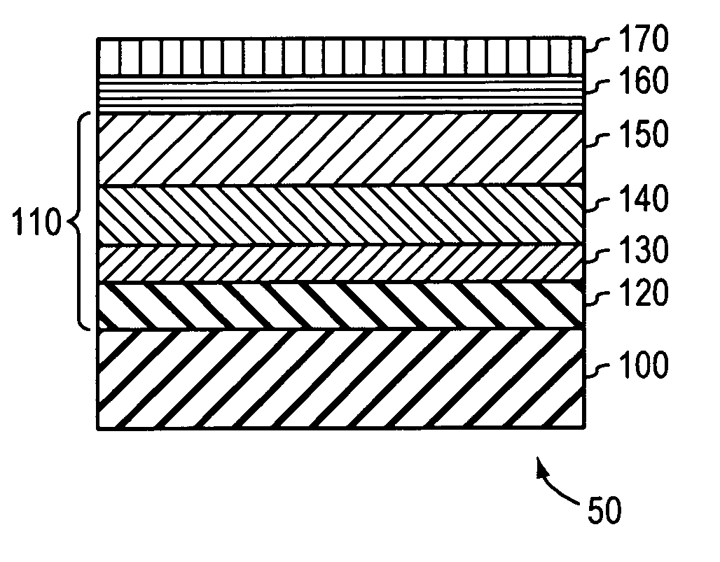
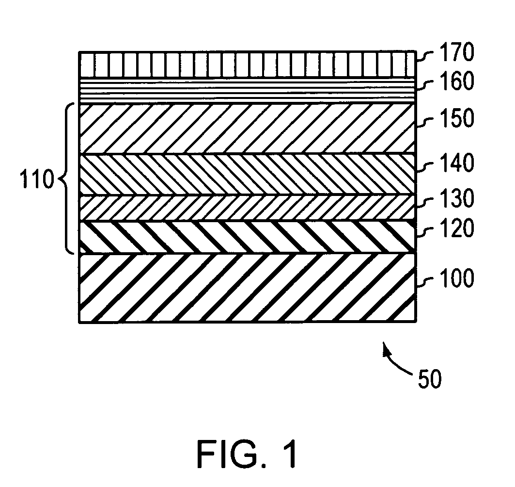
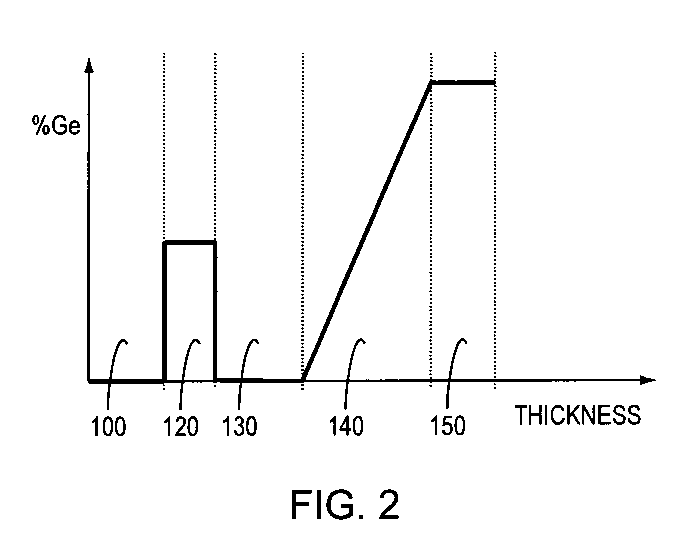
[0054] In accordance with various embodiments of the present invention, a semiconductor layer having a plurality of threading dislocations distributed substantially uniformly across its surface is used as a starting layer prior to the subsequent growth and relaxation of the compositionally graded layer and, optionally, as at least one intermediate layer during growth of the graded layer.

[0055] Referring to FIG. 1, a semiconductor structure 50 made in accordance with the embodiments of the invention includes a substrate 100. The substrate 100, suitable for use with the invention, comprises a semiconductor, such as silicon, silicon deposited over an insulator, such as, for example, SiO2, or a silicon-germanium alloy. In one embodiment, several semiconductor layers collectively referred to as layers 110 are epitaxially grown over the substrate 100. In this embodiment, the layers 110 and the substrate 100 may be referred to together as a “virtual substrate.”

[0056] The epitaxially grown...


PUM

PropertyMeasurementUnit
temperatureaaaaaaaaaa
thicknessaaaaaaaaaa

Abstract

Dislocation pile-ups in compositionally graded semiconductor layers are reduced or eliminated, thereby leading to increased semiconductor device yield and manufacturability. This is accomplished by introducing a semiconductor layer having a plurality of threading dislocations distributed substantially uniformly across its surface as a starting layer and / or at least one intermediate layer during growth and relaxation of the compositionally graded layer. The semiconductor layer may include a seed layer disposed proximal to the surface of the semiconductor layer and having the threading dislocations uniformly distributed therein.

Description

CROSS-REFERENCE TO RELATED APPLICATION [0001] This application claims the benefits of and priority to U.S. Provisional Application Ser. No. 60 / 405,484, filed on Aug. 23, 2002.FIELD OF THE INVENTION [0002] This application relates generally to semiconductor substrates and specifically to substrates comprising relaxed lattice-mismatched semiconductor layers. BACKGROUND [0003] The increasing operating speeds and computing power of microelectronic devices have recently given rise to the need for an increase in the complexity and functionality of the semiconductor structures that are used as the starting substrates in these microelectronic devices. Such “virtual substrates” based on silicon and germanium provide a platform for new generations of very large scale integration (“VLSI”) devices that exhibit enhanced performance when compared to devices fabricated on bulk Si substrates. Specifically, new technological advances enable formation of heterostructures using silicon-germanium alloy...

Claims


Application Information

Patent Timeline
Patent Type & Authority Applications(United States)
IPC IPC(8): H01L21/20C30B25/02C30B29/52H01L21/205H01L21/302H01L21/8238H01L31/0328
CPCC30B25/02C30B29/52H01L21/02381H01L21/0245H01L21/02505C30B25/183H01L21/02532H01L21/823807C30B23/066C30B23/025H01L21/0251H01L21/0262
Inventor LEITZ, CHRISTOPHERVINEIS, CHRISTOPHERWESTHOFF, RICHARDYANG, VICKYCURRIE, MATTHEW
Owner TAIWAN SEMICON MFG CO LTD
Why Eureka
Try Eureka