A multi-resistance memristor and its preparation method controlled by electric field and magnetic field
A multi-resistance, memristor technology with applications in field-controlled resistors, manufacturing/processing of electromagnetic devices, electrical components, etc.
- Summary
- Abstract
- Description
- Claims
- Application Information
AI Technical Summary
Problems solved by technology
Method used
Image

Examples
Embodiment 1
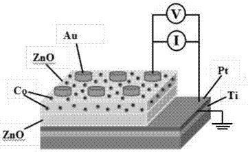
[0023] Such as figure 1 As stated above, an embodiment of the present invention provides a multi-resistance memristive device that is jointly regulated by an electric field and a magnetic field. The device is composed of a substrate, a resistive functional layer deposited on the substrate, and a top electrode. / SiO 2 / Si substrate, wherein the Pt layer on the substrate is used as the bottom electrode, the structure of the resistive switching functional layer is ZnO / ZnO-Co, and the top electrode is Au.
[0024] The preparation method of the multi-resistance state memristor controlled by the electric field and the magnetic field is as follows:
[0025] Step 1: Install a ZnO ceramic target with a purity of 99.99% and a Co metal target and an Au metal target with a purity of 99.99% as target materials in a magnetron sputtering chamber, with a size of 1×1cm 2 Pt / Ti / SiO 2 / Si substrate into the magnetron sputtering chamber, the background vacuum is lower than or equal to 8×10 -5...
Embodiment 2
[0033] Such as Figure 5 As mentioned above, the embodiment of the present invention provides a multi-resistance memristor device that is jointly regulated by an electric field and a magnetic field. / SiO 2 / Si commercial substrate, in which the Pt layer on the substrate is used as the bottom electrode, the resistive switch function layer structure is ZnO / ZnO-Co, and the top electrode is Pt.
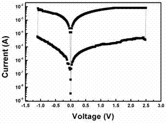
[0034] The bottom electrode is grounded, and when a certain positive voltage is applied to the top electrode, the device changes from a high-resistance state to a low-resistance state, and then when a certain negative voltage is applied to the top electrode, the device changes from a low-resistance state to a high-resistance state state.
[0035] The preparation method of the multi-resistance state memristor controlled by the electric field and the magnetic field is as follows:
[0036] Step 1: Install a ZnO ceramic target with a purity of 99.99% and a Co metal target and a Pt metal ta...
Embodiment 3
[0042] This embodiment provides a method for preparing a multi-resistance memristor that is jointly regulated by an electric field and a magnetic field, and the steps are as follows:
[0043] Step 1: Install a ZnO ceramic target with a purity of 99.99% and a Co metal target and a Pt metal target with a purity of 99.99% as target materials in a magnetron sputtering chamber, with a size of 1 × 1 cm 2 Pt / Ti / SiO 2 / Si substrate into the magnetron sputtering chamber, the background vacuum is lower than or equal to 8×10 -5 Pa.
[0044] The second step: high-purity Ar gas is used as the sputtering gas, and the Ar gas enters the sputtering chamber through the gas flow meter.
[0045] Step 3: Introduce Ar gas to keep the working pressure at 5-6 Pa, start the Co target and the ZnO target at the same time, and adjust the sputtering power of the Co target and the ZnO target to 20W and 50W respectively, and the sputtering pressure 0.8-2.0 Pa, the sputtering rate of Co is 0.048nm / s, and...
PUM
| Property | Measurement | Unit |
|---|---|---|
| thickness | aaaaa | aaaaa |
| thickness | aaaaa | aaaaa |
| thickness | aaaaa | aaaaa |
Abstract
Description
Claims
Application Information
 - R&D
- Intellectual Property
- Life Sciences
- Materials
- Tech Scout
- Unparalleled Data Quality
- Higher Quality Content
- 60% Fewer Hallucinations
Browse by: Latest US Patents, China's latest patents, Technical Efficacy Thesaurus, Application Domain, Technology Topic, Popular Technical Reports.
© 2025 PatSnap. All rights reserved.Legal|Privacy policy|Modern Slavery Act Transparency Statement|Sitemap|About US| Contact US: help@patsnap.com