Array substrate and display device

An array substrate and array substrate row technology are applied in the fields of array substrates and display devices, which can solve the problems of metal corrosion of display devices, and achieve the effects of avoiding metal corrosion problems and improving reliability.

Active Publication Date: 2019-06-07
BOE TECH GRP CO LTD +1
View PDF7 Cites 0 Cited by
  • Summary
  • Abstract
  • Description
  • Claims
  • Application Information

AI Technical Summary

Problems solved by technology

[0005] In order to overcome the defects in the above-mentioned prior art, the present invention provides an array substrate and a display device to solve the metal corrosion problem of the existing display device using GOA technology and improve its reliability

Method used


Image

  • Array substrate and display device
  • Array substrate and display device
  • Array substrate and display device

Examples


Embodiment Construction

[0031] As mentioned in the background, the existing display devices using the GOA technology have metal corrosion problems. The inventors of the present invention have found after research that one of the reasons for the aforementioned problems is:

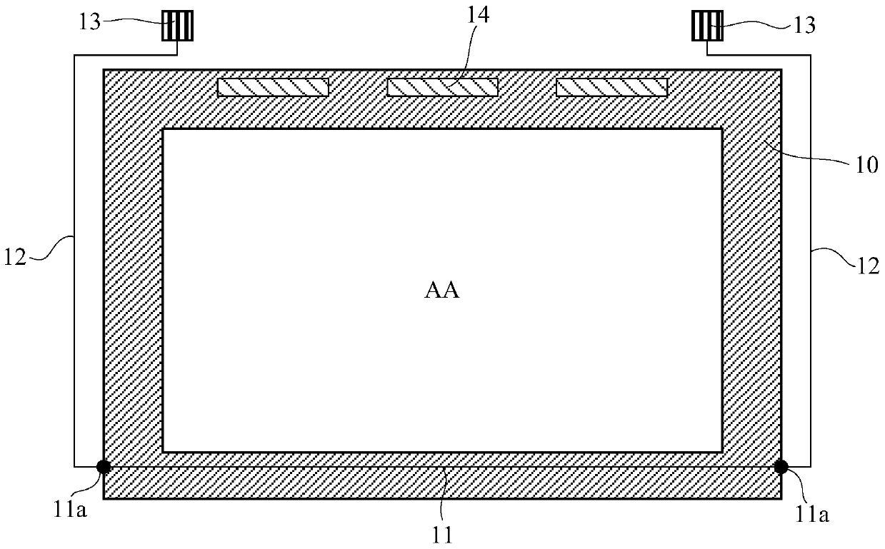
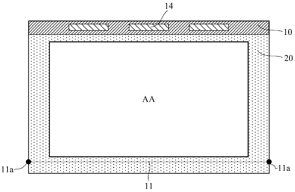
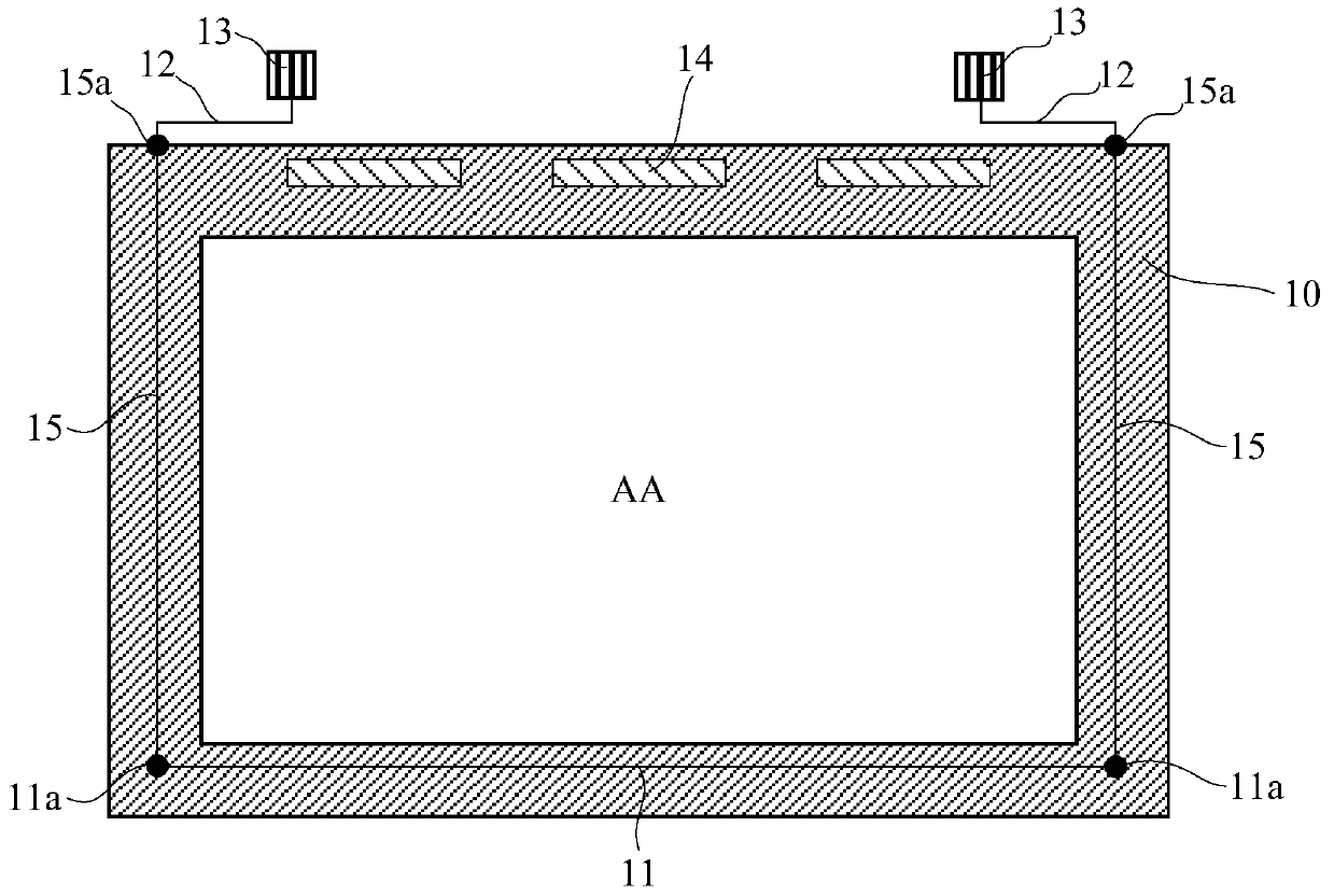
[0032] Such as figure 1 As shown, the array substrate 10 has a display area AA, GOA units (not shown) are arranged on the left and right sides outside the display area AA, and a data binding pad 14 is arranged on the outside of the display area AA, which is called a data binding pad. The side where 14 is located is the DP side of the array substrate 10 , the side opposite to the DP side is the DPO side of the array substrate 10 , and the two sides where the GOA unit is located are the GOA sides of the array substrate 10 .

[0033] In order to ensure product yield, in the final stage of the array substrate 10 manufacturing process, it is necessary to inspect the gate lines, data lines and other signal lines on the array substrate ...


PUM


Abstract

The invention provides an array substrate and a display device, which relate to the field of display technology and are used to solve the metal corrosion problem of the existing display device using the array substrate row driving technology and improve its reliability. Wherein, the array substrate includes a data line, a detection line and a lead-out line, the detection line is used to detect the data line, one end of the lead-out line is connected to the end of the detection line, and the other end Leading out from the data binding side of the array substrate, the two ends of the detection line are respectively connected to one of the lead-out lines. The aforementioned array substrate is used in a display device.

Description

technical field [0001] The present invention relates to the field of display technology, in particular to an array substrate and a display device. Background technique [0002] Array substrate row driving technology (hereinafter referred to as GOA technology, GOA stands for Gate Driver on Array in English) is a technology that integrates a gate driver on an array substrate. Compared with traditional COF (Chip On Film, chip-on-film) technology and COG (Chip on Glass, chip bonded on glass) technology, GOA technology reduces the use of gate drive chips, which can reduce power consumption and cost , and the GOA technology eliminates the bonding process in the gate direction, which is conducive to the improvement of production capacity. [0003] The basic structure of the array substrate using GOA technology is as follows: the array substrate has a display area, and a plurality of horizontal gate lines and a plurality of vertical data lines are arranged inside the display area; ...

Claims


Application Information

Patent Timeline
Patent Type & Authority Patents(China)
IPC IPC(8): G02F1/1362H01L27/32
CPCG02F1/1362G02F1/136286G02F1/136254H10K59/131
Inventor 江鹏贾纬华马小叶杨海鹏戴珂尹傛俊王章涛
Owner BOE TECH GRP CO LTD
Why Eureka
Try Eureka