PCIE SSD array data writing method and system

A data writing and array technology, applied in the direction of input/output to record carrier, etc., can solve problems such as memory performance array performance bottlenecks, and achieve the effect of improving performance

Active Publication Date: 2015-12-30
HUNAN GOKE MICROELECTRONICS
View PDF4 Cites 2 Cited by
  • Summary
  • Abstract
  • Description
  • Claims
  • Application Information

AI Technical Summary

Problems solved by technology

For example, the theoretical write bandwidth of an array composed of 48 Intel p3700 solid-state drives can r

Method used


Image

  • PCIE SSD array data writing method and system
  • PCIE SSD array data writing method and system
  • PCIE SSD array data writing method and system

Examples


Embodiment Construction

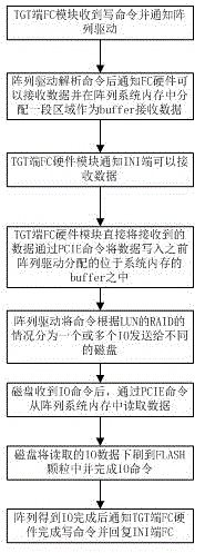
[0032] The present invention is based on a storage array using PCIESSD as a storage medium, and PCIESSD includes but not limited to SSD disks based on AHCI and NVMe protocols.

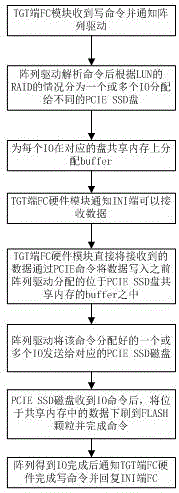
[0033] The present invention needs to share the memory of the PCIESSD disk to the host (the host of the SSD disk). At present, the NVMe1.2 protocol has included the interface for sharing the disk memory to the host. Other PCIESSD disks that do not support the NVMe1.2 protocol can also be customized The extended protocol realizes sharing the memory of the disk controller with the host.

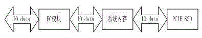
[0034] From figure 2 It can be seen that the biggest difference between the present invention and the existing solutions is that the data is directly transmitted from the FC module to the shared memory of the PCIe SSD disk controller without passing through the system memory, thereby avoiding the performance of the system memory from becoming the bottleneck of the array performance. Each PCI ESSD disk has its own memo...


PUM


Abstract

The invention discloses a PCIE SSD array data writing method and system. Data is directly transmitted from an FC module to a shared memory of a PCIE SSD disk controller without passing through the system memory. Therefore, the system memory cannot become the bottleneck restricting the array performance. In addition, as each PCIE SSD disk is provided with a memory, the memory performance of a disk cannot become the bottleneck restricting the array and disk performance so long as the write performance of the memory on each disk is twice of the write bandwidth of the disk per se.

Description

technical field [0001] The invention relates to a data writing method and system of a PCIESSD array. Background technique [0002] The existing operating systems and disk array solutions are designed according to the fact that the performance of mechanical disks is much lower than that of memory. Compared with the read and write delays of mechanical disks, the read and write delays of memory are almost negligible, so regardless of Whether it is a commonly used operating system or the software architecture of the array, the written data is first placed in the system memory and then sent to the disk or returned to the application. Let's take a look at the read and write process of the current architecture in the case of common disk arrays sharing LUNs to hosts through FC, see figure 1 . [0003] figure 1 The method does not consider the write-back situation, the IO data is first written to the array system memory and then returned to the requester. This solution can greatl...

Claims


Application Information

Patent Timeline
IPC IPC(8): G06F3/06
Inventor 王翔向平周士兵姜黎马翼田达海彭鹏
Owner HUNAN GOKE MICROELECTRONICS
Why Eureka
Try Eureka