Display panel and manufacturing method thereof

A technology of display panel and manufacturing method, which is applied in identification devices, semiconductor/solid-state device parts, instruments, etc., to achieve the effect of reducing defective ratio, reducing probability of scratches, and reducing influence

Inactive Publication Date: 2016-01-06
BOE TECH GRP CO LTD +1
View PDF6 Cites 13 Cited by
  • Summary
  • Abstract
  • Description
  • Claims
  • Application Information

AI Technical Summary

Problems solved by technology

[0005] The main purpose of the present invention is to provide a display panel and its manufacturing method, aiming to solve the technical problem of how to control the reduction of glass debris in the manual operation process to reduce the probability of scratching the IC

Method used


Image

  • Display panel and manufacturing method thereof
  • Display panel and manufacturing method thereof
  • Display panel and manufacturing method thereof

Examples


Embodiment Construction

[0020] The following will clearly and completely describe the technical solutions in the embodiments of the present invention with reference to the accompanying drawings in the embodiments of the present invention. Obviously, the described embodiments are only part of the embodiments of the present invention, not all of them. Based on the embodiments of the present invention, all other embodiments obtained by persons of ordinary skill in the art without making creative efforts belong to the protection scope of the present invention.

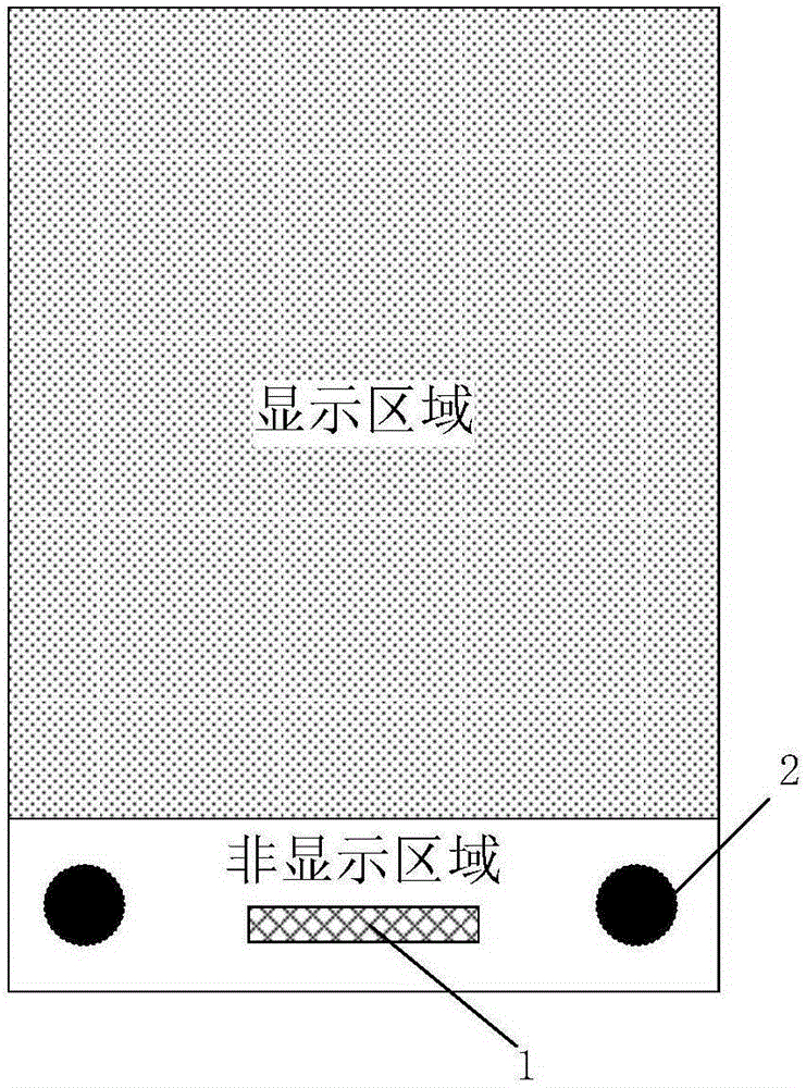
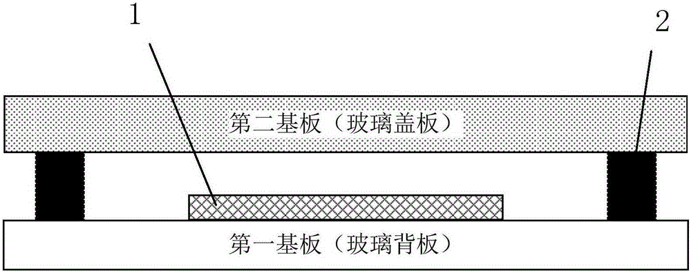
[0021] The main purpose of the present invention is to solve the problem that when the IC side glass is peeled off by manual operation in the POST process, the manual operation itself is easy to cause scratches to the IC in the non-display area of ​​the Panel, and proposes a method of applying Frit glue on both sides of the IC. (Glass glue) design method, so that the package glass and the backplane glass are hollowed out above and around the IC, s...


PUM

PropertyMeasurementUnit
diameteraaaaaaaaaa

Abstract

The invention discloses a display panel and a manufacturing method thereof. The display panel comprises a first substrate and a second substrate, and the first substrate and the second substrate are in opposite arrangement. An IC (integrated circuit) is arranged in a non-display region of the first substrate, and supporting parts higher than the IC are arranged in an area, except for the area with the IC, of the non-display region. Therefore, the IC can be protected from being scratched to the maximal extent, and yield of a whole backlight module is increased.

Description

technical field [0001] The present invention relates to the field of display technology, in particular to a display panel and a manufacturing method thereof. Background technique [0002] The cutting (POST) process is to cut a whole piece of glass (Q-Glass) into multiple small pieces of glass (Panel). Please refer to figure 1 , figure 1 It is a schematic diagram of cutting a display panel into sub-display panels according to the prior art, such as figure 1 As shown, Q-Glass needs to be cut into 50 small Panels (labeled AA-EK). First, the Q-Glass is cut into 5 rows (ie, row A, row B, row C, row D, and row E). Next, cut each row into 10 panels. For row A, it includes AA-AJ. At the same time, the cover glass at the position of the dotted line box needs to be cut off to expose the position of the ICTeg area, where Teg input and IC input It is two different signal giving methods, Teg is the input terminal of ET lighting signal for yield statistics, and IC is the input termin...

Claims


Application Information

Patent Timeline
Patent Type & Authority Applications(China)
IPC IPC(8): G09F9/00G02F1/1333
CPCG02F1/133351G09F9/00G02F1/1339G02F1/13452H10K50/8428H01L23/053H01L23/08H01L23/13H01L23/15H01L23/24
Inventor 杨凡郭坤杨玉清刘祺张博陈飞承天一李子华吴岩杨津彭利满孔超
Owner BOE TECH GRP CO LTD
Why Eureka
Try Eureka