An etching device and a single-side etching method of a wafer

An etching device and wafer technology, which is applied in the fields of electrical components, semiconductor/solid-state device manufacturing, circuits, etc., can solve the problems of scrapping wafers, adding protective layers, and increasing the production cost of semiconductor chips.

Active Publication Date: 2018-08-24
ZHUZHOU CRRC TIMES SEMICON CO LTD
View PDF5 Cites 0 Cited by
  • Summary
  • Abstract
  • Description
  • Claims
  • Application Information

AI Technical Summary

Problems solved by technology

[0003] However, the disadvantage of the single-side etching method of the wafer is that it is necessary to increase the process of coating or growing a protective layer on the surface of the wafer, which reduces the production efficiency of the semiconductor chip, and the protective layer is formed on the surface of the wafer. There is a risk of peeling off or peeling off when the wafer is immersed in the corrosive liquid, and once the protective layer is peeled off or peeled off, the wafer will be scrapped, thereby increasing the production cost of the semiconductor chip

Method used


Image

  • An etching device and a single-side etching method of a wafer
  • An etching device and a single-side etching method of a wafer
  • An etching device and a single-side etching method of a wafer

Examples


Embodiment Construction

[0041] As mentioned in the background, when the wafer is etched by wet method in the prior art, the efficiency is low and the cost is high.

[0042] In view of this, an embodiment of the present invention provides an etching device, which is applied to wafer wet etching, including:
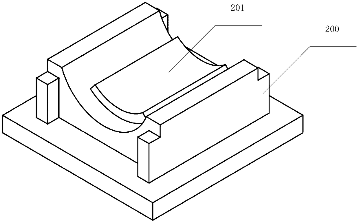
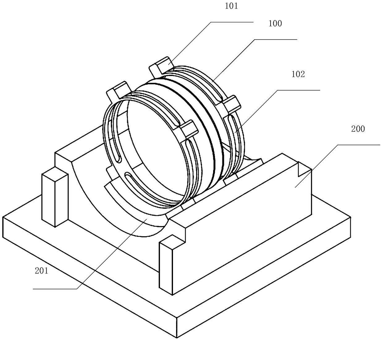
[0043] base;

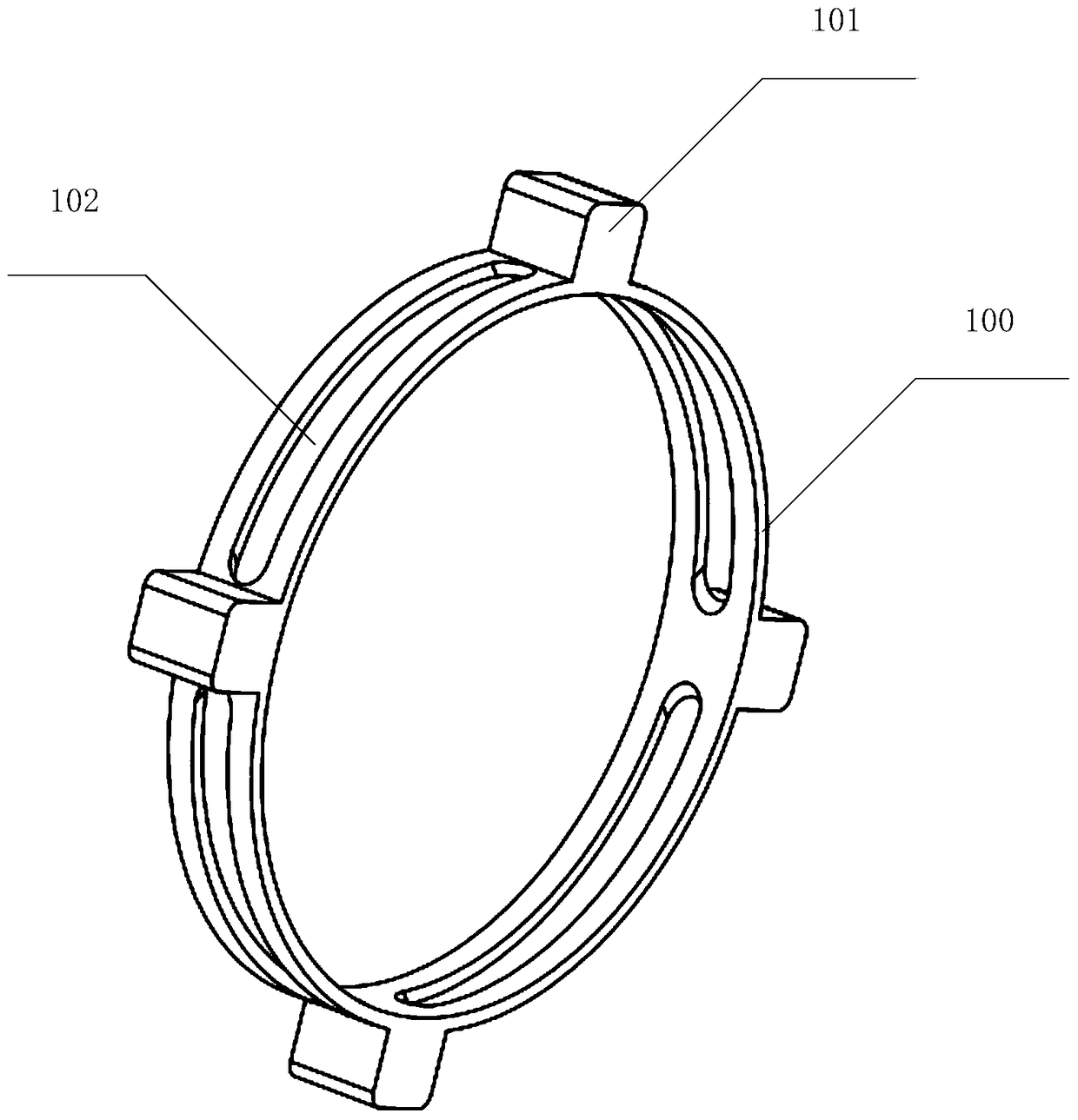
[0044] A plurality of clip rings arranged on the base, at least two wafers are placed between adjacent clip rings, and the surface to be etched of the wafer faces the adjacent clip rings , and the clip ring is circular, and its side wall includes at least one liquid inlet groove;

[0045] A clamping device arranged on the base, the clamping device is used for clamping a plurality of clip rings and a plurality of wafers placed on the base.

[0046] Correspondingly, the embodiment of the present invention also provides a single-side etching method of a wafer, which is applied to the etching device described in the above embodiment, including:

[0047] placing a plurality of said cl...


PUM


Abstract

The application discloses an etching device and a wafer one side etching method. The base of the etching device is used for placing a plurality of clamping piece rings; at least two wafers are arranged between adjacent clamping piece rings; the water surfaces to be etched are towards adjacent clamping piece rings; the plurality of clamping piece rings and the plurality of wafers arranged on the base are clamped by a clamping device, and then corrosive liquids can be injected through the liquid inlet slots of the clamping piece rings to corrode the wafers. At least two wafers are closely attached, and only the water surfaces to be etched are towards adjacent clamping piece rings, and thereby after the corrosive liquids are injected through the liquid inlet slots of the clamping piece rings, the corrosive liquids can only touch the water surfaces to be etched, thereby etching one side of a wafer.

Description

technical field [0001] The invention belongs to the field of semiconductor devices, and more specifically relates to an etching device and a single-side etching method of a wafer. Background technique [0002] Wafer is the basic material for manufacturing semiconductor chips. In the manufacturing process of semiconductor chips, it is necessary to etch the wafer on one side. Wet etching is easy to operate, requires less equipment, and is easy to realize large-scale The advantages of mass production and less damage to the wafer have become the mainstream single-side etching method. In the prior art, before performing single-sided etching of the wafer, it is necessary to coat or grow a protective layer on the side that does not need to be etched, and then immerse the wafer with the protective layer in an etching liquid The surface to be etched is etched, and finally the wafer is taken out, the protective layer is removed and cleaned, and the single-side etching of the wafer is...

Claims


Application Information

Patent Timeline
Patent Type & Authority Patents(China)
IPC IPC(8): H01L21/67H01L21/306
CPCH01L21/30604H01L21/67086
Inventor 王东东王政英邹冰艳刘芹唐革郭润庆刘锐鸣高军刘应姚震洋
Owner ZHUZHOU CRRC TIMES SEMICON CO LTD
Why Eureka
Try Eureka