

Method for forming double mosaic structures
A dual damascene structure and graphics technology, which is applied in the fields of electrical components, semiconductor/solid-state device manufacturing, circuits, etc., can solve the problems of poor performance of the dual damascene structure
- Summary
- Abstract
- Description
- Claims
- Application Information
AI Technical Summary
Problems solved by technology
Method used
Image

Examples
Embodiment Construction
[0042] After research and discovery, the reasons for the poor performance of the dual damascene structure formed by the method of the prior art are as follows:
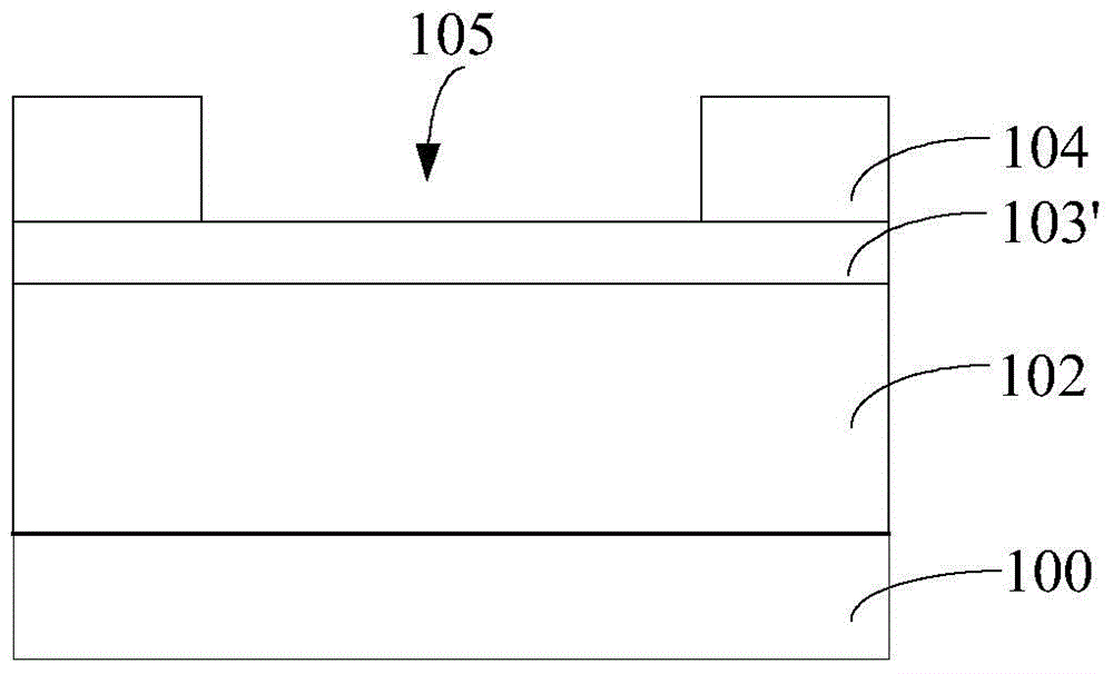
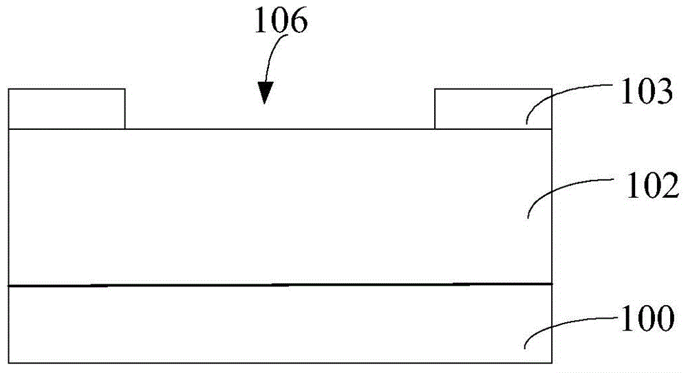
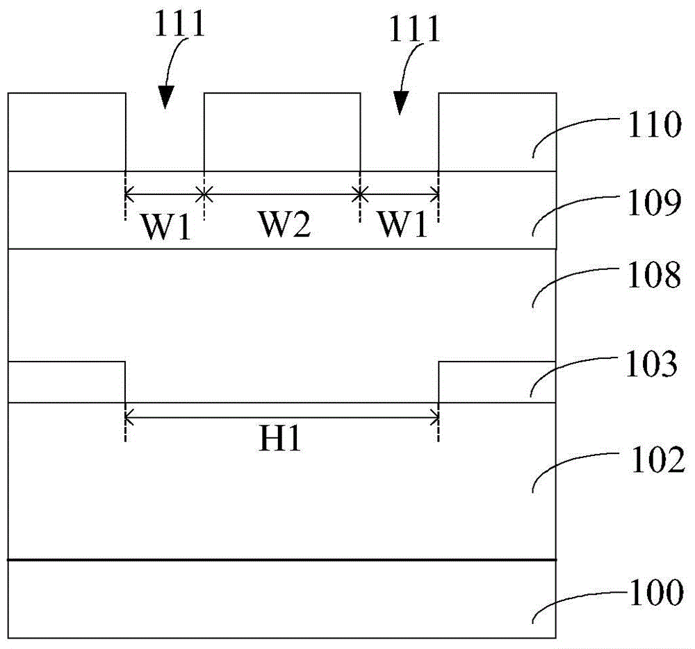
[0043] refer to image 3 The width H1 of the second opening 106 in the titanium nitride layer 103 is equal to the sum of the width W1 of the two third openings 111 and the width W2 of the photoresist between the two adjacent third openings 111 . refer to Figure 5 After forming two first through holes 112 in the low-k dielectric layer 102, the second opening 106 is exposed at the sidewall of one of the first through holes 112 (refer to figure 2 ) of one side wall; the other side wall of the first through hole 112 also exposes the other side wall of the second opening 106 . That is, from Figure 5As shown in the sectional view, one side wall boundary of the second opening 106 is on the same straight line as the side wall boundary of a first through hole 112, and the other side wall boundary of the second opening 10...
PUM
 Abstract
Description
Claims
Application Information