Supercharge Your Innovation With Domain-Expert AI Agents!

Semiconductor structure and forming method thereof

A semiconductor and precursor technology, applied in the field of semiconductor structure and its formation, can solve the problems of great impact on performance, decline in electrical performance and reliability performance of semiconductor structure, small size, etc., to improve electrical performance and reliability performance, improve Time-dependent breakdown performance, the effect of improving the blocking effect

Active Publication Date: 2019-01-15
SEMICON MFG INT (SHANGHAI) CORP +1
View PDF9 Cites 0 Cited by
  • Summary
  • Abstract
  • Description
  • Claims
  • Application Information

AI Technical Summary

Problems solved by technology

With the advancement of technology nodes, the size of the interconnection structure has become smaller and smaller; correspondingly, the process of forming the interconnection structure has become more and more difficult, and the formation quality of the interconnection structure has a great impact on the back end (Back End OfLine , BEOL) The performance of the circuit is greatly affected, and in severe cases, it will affect the normal operation of the semiconductor device
[0004] However, the formation process of the interconnection structure in the prior art easily leads to a decrease in the electrical performance and reliability of the semiconductor structure

Method used


Image

  • Semiconductor structure and forming method thereof
  • Semiconductor structure and forming method thereof
  • Semiconductor structure and forming method thereof

Examples


Embodiment Construction

[0034] It can be seen from the background art that with the continuous development of integrated circuit manufacturing technology, the interconnection process has been widely used in the back-end process. Among them, since metal copper has a lower resistivity and has stronger resistance to electromigration (Electromigration), the back-end interconnection process mainly uses copper interconnection.

[0035] However, the formation process of the copper interconnection easily leads to the degradation of the electrical performance and reliability performance of the semiconductor structure. Combining with a method for forming a semiconductor structure, the reasons for the degradation of the electrical performance and reliability of the semiconductor structure are analyzed.

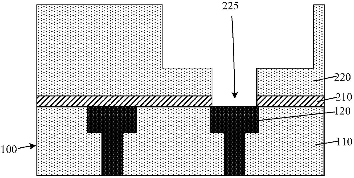
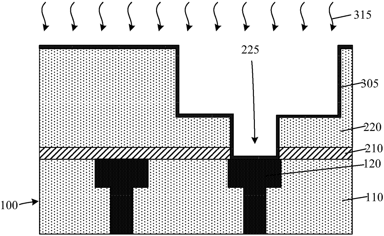
[0036] The forming method includes: providing a base, on which a dielectric layer is formed, and an opening exposing the base is formed in the dielectric layer; forming a barrier layer on the bottom and side wa...


PUM

PropertyMeasurementUnit
relative permittivityaaaaaaaaaa

Abstract

A method for for a semiconductor structure includes provide a substrate, forming a dielectric layer on that substrate, and forming an opening in the dielectric lay exposing the substrate; Forming a barrier layer on the bottom and side walls of the opening by an atomic layer deposition process, and doping Ge ions in the barrier layer; After forming the barrier layer doped with Ge ions, a copper interconnect electrically connected to the substrate is formed in the opening. As that barry layer is dope with Ge ions, after the copper interconnect is for in the opening, Ge in the barrier layer can form Cu Ge bond, so as to improve the barrier effect of the barrier layer on copper, improve the problem of copper diffusion, and further improve the electrical performance and reliability performanceof the semiconductor structure, for example, the breakdown performance over time can be improved.

Description

technical field [0001] The invention relates to the field of semiconductor manufacturing, in particular to a semiconductor structure and a forming method thereof. Background technique [0002] With the continuous development of integrated circuit manufacturing technology, people's requirements for the integration and performance of integrated circuits are becoming higher and higher. In order to improve integration and reduce costs, the critical dimensions of components are getting smaller and the circuit density inside integrated circuits is increasing. This development makes the surface of the wafer unable to provide enough area to make the required interconnection lines. [0003] In order to meet the requirements of the interconnection line after the critical dimension is reduced, at present, the conduction between different metal layers or the metal layer and the substrate is realized through the interconnection structure. With the advancement of technology nodes, the si...

Claims


Application Information

Patent Timeline
Patent Type & Authority Applications(China)
IPC IPC(8): H01L21/768
CPCH01L21/76822H01L21/76825H01L21/76843
Inventor 邓浩
Owner SEMICON MFG INT (SHANGHAI) CORP
Features
  • R&D
  • Intellectual Property
  • Life Sciences
  • Materials
  • Tech Scout
  • Unparalleled Data Quality
  • Higher Quality Content
  • 60% Fewer Hallucinations
Learn More