
Copper indium gallium selenium thin film solar cell provided with aluminum nitride (AIN) thin film layer

A technology of thin-film solar cells and copper indium gallium selenide, applied in circuits, photovoltaic power generation, electrical components, etc., can solve the problems of high equipment investment intensity, expensive raw materials, unfavorable solar cells, etc., to reduce production equipment investment and improve horizontal Uniformity, the effect of improving the overall performance

Inactive Publication Date: 2012-07-04
NANKAI UNIV
View PDF5 Cites 33 Cited by
  • Summary
  • Abstract
  • Description
  • Claims
  • Application Information

AI Technical Summary

Problems solved by technology

This technology is applied to the production and preparation of large-area thin-film solar cells. Not only is the equipment investment intensive, but also the raw materials are expensive, which is not conducive to reducing the cost of solar cells.

Method used


Image

  • Copper indium gallium selenium thin film solar cell provided with aluminum nitride (AIN) thin film layer
  • Copper indium gallium selenium thin film solar cell provided with aluminum nitride (AIN) thin film layer
  • Copper indium gallium selenium thin film solar cell provided with aluminum nitride (AIN) thin film layer

Examples


Embodiment 1

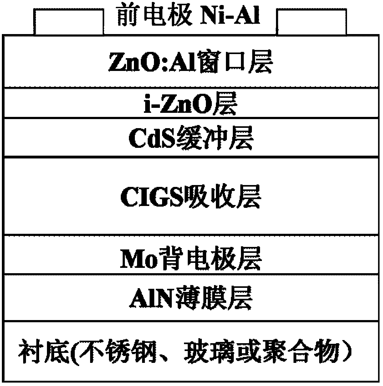
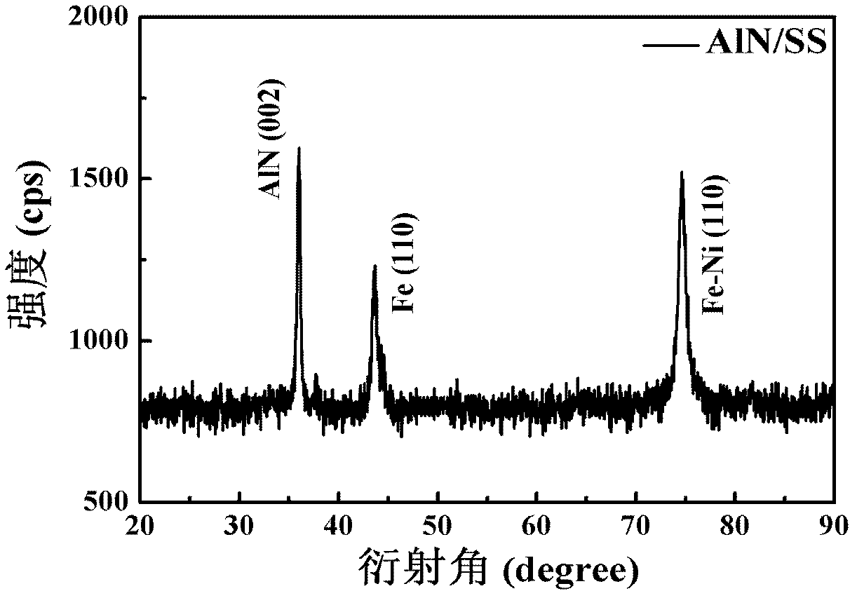
[0031]A kind of copper indium gallium selenium thin film solar cell with AlN thin film layer, see figure 1 , using stainless steel as the substrate and using magnetron sputtering to prepare an AlN film as an electrically insulating impurity barrier layer, the preparation steps are as follows:

[0032] 1) The 0.05 μm stainless steel foil (SS) is ultrasonically cleaned, dehydrated and dried, then placed in the vacuum chamber of the magnetron sputtering deposition system, dehydrated and degassed;

[0033] 2) The AlN film was prepared on the stainless steel substrate by magnetron sputtering, and the process parameters: the background vacuum was 3×10 -3 Pa, the substrate temperature is 150°C, the target distance of the metal Al target is 60mm, and the Ar and N 2 The flow rate of the mixed gas is 25sccm, Ar and N 2 The volume ratio is 1.5:1, the working gas pressure in the vacuum chamber is 0.5Pa, and the sputtering power density is 1.2W / cm 2 , the thickness of the prepared AlN f...

Embodiment 2

[0043] A kind of copper indium gallium selenium thin film solar cell with AlN thin film layer, see Figure 4 , using stainless steel as a substrate to prepare AlN / Cr composite film as an electrical insulation and impurity barrier layer, the preparation steps are as follows:

[0044] 1) The 0.05 μm stainless steel foil (SS) is ultrasonically cleaned, dehydrated and dried, then placed in the vacuum chamber of the magnetron sputtering deposition system, dehydrated and degassed;

[0045] 2) The Cr film was prepared on the stainless steel substrate by magnetron sputtering, and the process parameters: the background vacuum was 3×10 -3 Pa, the flow rate of Ar is 15sccm, the target-base distance is 60mm, the working gas pressure of the vacuum chamber is 0.8Pa, and the sputtering power density is 0.8W / cm 2 , the thickness of the prepared Cr film is 500nm, and the same method as in Example 1 is used to prepare an AlN film with a thickness of 200nm on the Cr film, and then AlN / Cr / SS is ...

Embodiment 3

[0049] A copper indium gallium selenium thin film solar cell with an AlN thin film layer is prepared with glass as a substrate to prepare an AlN thin film as an impurity barrier and stress transition layer, see figure 1 , the preparation steps are as follows:

[0050] 1) Ultrasonic cleaning is performed on a 2mm glass substrate, dehydrated and dried, and then placed in a vacuum chamber of a magnetron sputtering deposition system for dehydration and degassing;

[0051] 2) Prepare AlN thin film on glass substrate by magnetron sputtering, process parameters: background vacuum is 3×10 -3 Pa, the substrate temperature is 300°C, the target distance of the metal Al target is 60mm, and the Ar and N 2 The flow of mixed gas is 30sccm, Ar and N 2 The volume ratio is 1:1, the working gas pressure in the vacuum chamber is 1Pa, and the sputtering power density is 1.2W / cm 2 , the thickness of the prepared AlN film is 0.5 μm;

[0052] 3) A low-pressure single-layer Mo back electrode was p...


PUM

PropertyMeasurementUnit
thicknessaaaaaaaaaa
thicknessaaaaaaaaaa
thicknessaaaaaaaaaa

Abstract

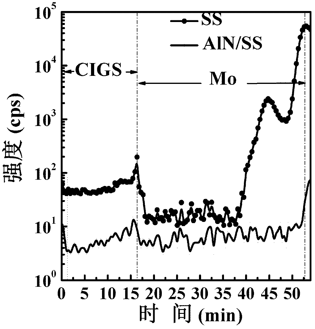
A copper indium gallium selenium (CIGS) thin film solar cell provided with an aluminum nitride (AIN) thin film layer comprises a substrate, a molybdenum (Mo) back electrode layer, a CIGS absorbed layer, a cadmium dating sulphide (CdS) buffer layer, an intrinsic zinc oxide (i-ZnO) layer, a mixing zinc oxide (ZnO:AI) window layer and front electrode nickel aluminum. The AIN thin film layer is arranged between the substrate and the Mo back electrode layer and serves as an electric insulation impurity barrier layer when the substrate is made of metal, the AIN thin film layer serves as an impurity barrier and stress intermediate layer when the substrate is made of glass, and the AIN thin film layer serves as a heat buffer layer when the substrate is made of polymer. The thin film solar cell has the advantages of adopting simple and cheap magnetic control sputtering technology to prepare an AIN thin film to serve as the impurity barrier layer or the electrical insulating layer of the substrate, being capable of having good resisting effects and keeping insulation characteristics of metal atoms even through the solar cell is prepared at high substrate temperature, and providing prerequisite conditions for manufacturing inline type tinsel substrate thin film solar cells.

Description

technical field [0001] The invention relates to a copper indium gallium selenide thin film solar cell, in particular to a copper indium gallium selenide thin film solar cell provided with an AlN thin film layer. Background technique [0002] Flexible substrate copper indium gallium selenide (CIGS for short) thin film solar cell is a solar cell composed of several layers of semiconductor thin film and metal thin film deposited by vacuum deposition and chemical method on metal foil or polymer film substrate. Because of its light weight, foldability, non-fragility, good mechanical properties, high power-to-weight ratio, good space performance, and can be produced by a low-cost tape-to-roll deposition process, it has a huge market prospect. Commonly used flexible substrate materials include: metal substrates such as stainless steel foil (SS), Al foil, Mo foil, Cu foil, Ti foil, etc., and polymer material substrates such as polyimide (PI) films. Because the metal substrate still...

Claims


Application Information

Patent Timeline
Patent Type & Authority Applications(China)
IPC IPC(8): H01L31/0352H01L31/0304H01L31/04H01L31/0445
CPCY02E10/50
Inventor 张毅李博研孙云周志强刘玮
Owner NANKAI UNIV
Learn More