Method for forming semiconductor structure

A semiconductor and wet etching technology, applied in semiconductor/solid-state device manufacturing, electrical components, circuits, etc., can solve problems such as difficulty in adjusting the performance of transistors

Active Publication Date: 2016-01-06
SEMICON MFG INT (SHANGHAI) CORP
View PDF3 Cites 6 Cited by
  • Summary
  • Abstract
  • Description
  • Claims
  • Application Information

AI Technical Summary

Problems solved by technology

[0009] However, with the development of semiconductor technology, the size of semiconductor devices is gradually shrinking, and it is more difficult to adjust the performance of transistors.

Method used


Image

  • Method for forming semiconductor structure
  • Method for forming semiconductor structure
  • Method for forming semiconductor structure

Examples


Embodiment Construction

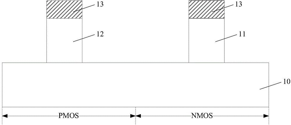
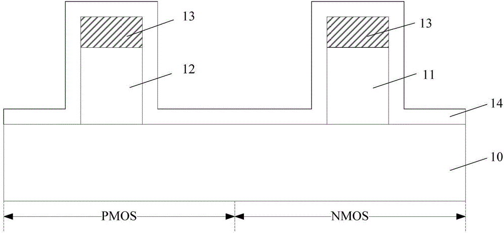
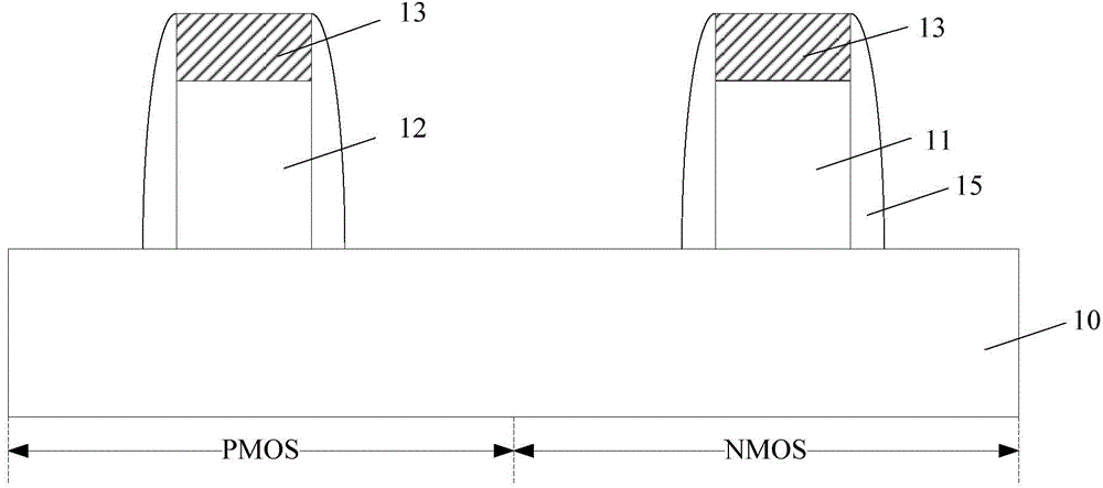
[0037] As mentioned in the background art, in the prior art, the sidewalls on the gate sidewall surfaces of different transistors are usually formed at the same time, so that the thickness of the gate sidewalls of different transistors is the same, and it is impossible to make a judgment on the performance of different transistors through the thickness of the sidewalls. Adjustment. In order to accurately adjust the performance of different transistors, it is necessary to form sidewalls with different thicknesses for different transistors to meet the requirements of device design. For example, since the diffusion rate of the dopant ions in the source and drain of the PMOS transistor is greater than the diffusion rate of the dopant ions in the source and drain of the NMOS transistor, in order to prevent the source and drain of the PMOS transistor from punching through, it is necessary to make the gate of the PMOS transistor The thickness of the pole sidewall is greater than the ...


PUM


Abstract

The invention provides a method for forming a semiconductor structure. The method comprises the steps of providing a semiconductor substrate comprising a first region and a second region, forming a first grid dielectric layer on the first region and a first grid on the surface of the first grid dielectric layer, forming a second grid dielectric layer on the second region and a second grid on the surface of the second grid dielectric layer, forming a first dielectric layer that covers the semiconductor substrate, the first grid dielectric layer, the first grid, the second grid dielectric layer and the second grid, forming a protective layer on the surface of the first dielectric layer, forming a mask layer on the second region, removing the protective layer on the first region with the mask layer as a mask, removing the first dielectric layer on the first region after the removal of the mask layer, forming a second dielectric layer on the first region and the second region after the removal of the first dielectric layer from the first region, and etching the second dielectric layer till reaching the surface of the semiconductor substrate so as to form a first side wall and a second side wall. Based on the above method, side walls of different thicknesses are formed on different transistors, so that the performances of the transistors are adjusted.

Description

technical field [0001] The invention relates to the technical field of semiconductors, in particular to a method for forming a semiconductor structure. Background technique [0002] Sidewalls are formed on the side walls of the gate of metal oxide semiconductor (MOS) transistors. On the one hand, the sidewalls can protect the gate, and on the other hand, they can also limit the distance between the source and drain and the gate, so as to avoid the source The dopant ions in the drain diffuse too deeply into the channel region, resulting in problems such as source-drain breakthrough. [0003] Usually, after the gate of the transistor is formed, spacers are first formed on the surface of the sidewall of the gate, and then lightly doped ion implantation is performed on the semiconductor substrate on both sides of the gate to form a lightly doped region to improve the short channel of the transistor. To achieve the channel effect, the semiconductor substrate on both sides of the...

Claims


Application Information

Patent Timeline
Patent Type & Authority Applications(China)
IPC IPC(8): H01L21/8238
Inventor 刘格致
Owner SEMICON MFG INT (SHANGHAI) CORP
Why Eureka
Try Eureka