Burn-in board

A technology for burn-in boards and substrates, applied in instruments, measuring devices, measuring electronics, etc., can solve problems such as loss of accessories, long time-consuming plugging and unplugging processes, and reduced work efficiency

Active Publication Date: 2016-01-13
FOUNDER MICROELECTRONICS INT
View PDF7 Cites 1 Cited by
  • Summary
  • Abstract
  • Description
  • Claims
  • Application Information

AI Technical Summary

Problems solved by technology

In this kind of sample method: the plugging and unplugging process of accessories takes a long time, which reduces work efficiency; and usually in order to ensure good contact of the aging boa

Method used


Image

  • Burn-in board
  • Burn-in board
  • Burn-in board

Examples


Embodiment Construction

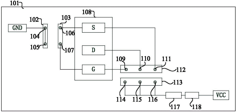
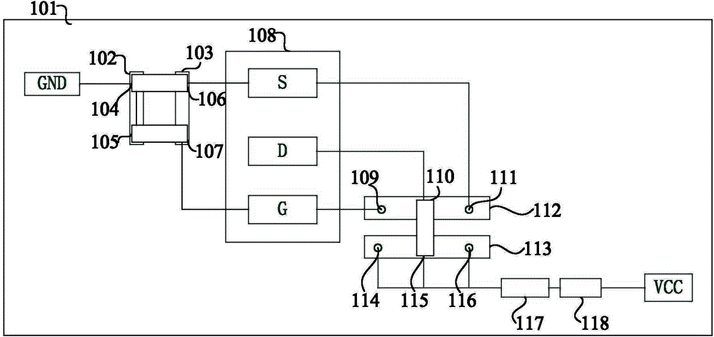
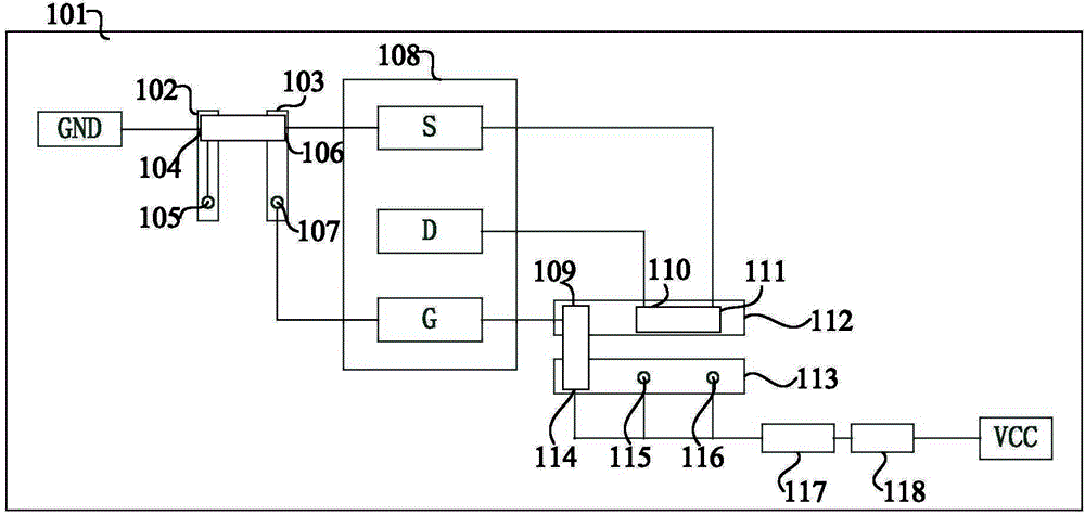
[0025] The burn-in board provided by the embodiment of the present invention includes: a substrate, on which a socket for plugging in a device under test and a first to fourth row of pins are provided. The socket includes a source S port, a drain D port, and a gate. G port; the first pin and the second pin on the first row of pins are connected, and the first pin or the second pin is grounded; the first pin on the second row of pins is connected to the S port, and the second pin is connected to the G port; third The first pin to the third pin on the pin header are respectively connected to the G port, the D port and the S port; the first pin to the third pin on the fourth pin are all connected to VCC; the first pin and the second pin of the first pin The stitches are respectively opposite to the first stitch and the second stitch of the second row of needles, and the first to third pins of the third row of needles are respectively opposite to the first to third stitches of the f...


PUM


Abstract

The embodiment of the invention relates to the technical field of semiconductor chip quality reliability, and especially relates to a burn-in board which is simple to operate and highly universal. According to the embodiment of the invention, a first pin and a second pin on a first pin header are communicated, and the first pin or the second pin is grounded; a first pin on a second pin header is communicated with a port S, and a second pin is communicated with a port G; a first pin, a second pin and a third pin on a third pin header are respectively communicated with the port G, a port D and the port S; and a first pin, a second pin and a third pin on a fourth pin header are communicated with VCC. Any of the port S, the port D and the port G can be grounded or connected to a power source by plugging a short-circuit cap onto the pin headers, so that a variety of experiments can be conducted by changing the plugging of the short-circuit cap, and the universality of the burn-in board is further improved.

Description

Technical field [0001] The invention relates to the technical field of semiconductor chip quality reliability, in particular to an aging board. Background technique [0002] With the continuous development of semiconductor technology, the application fields of chips have begun to continue to extend, and the reliability requirements for chips have become higher and higher. In order to ensure the reliability of the chip, the chip is usually burn-in test (Burn-inTest), that is, after the chip is manufactured, the chip is often mounted on a burn-in board. At high temperatures, it is generally 150 for silicon devices. ℃ and above, make the chip expose the defects in the device as soon as possible, so as to detect defective devices. [0003] At present, the general burn-in board in the industry needs to analyze the failure mode of the chip by plugging and unplugging accessories (jumpers, resistors) on the burn-in board. In this sample method: the plugging and unplugging process of acce...

Claims


Application Information

Patent Timeline
IPC IPC(8): G01R1/04G01R31/27
Inventor 徐娟曹婷
Owner FOUNDER MICROELECTRONICS INT
Why Eureka
Try Eureka