touch display device

A technology of touch display and touch sensing, which is applied in the fields of instruments, computing, and electrical digital data processing, and can solve problems such as poor conductivity, affecting electronic components, and affecting electrical signal transmission of touch sensing modules.

Inactive Publication Date: 2019-02-12
INTERFACE OPTOELECTRONICS SHENZHEN +1
View PDF4 Cites 0 Cited by
  • Summary
  • Abstract
  • Description
  • Claims
  • Application Information

AI Technical Summary

Problems solved by technology

It is true that installing an electrostatic protection component can quickly discharge part of the accumulated electrostatic charge, but because the material of the protective layer is usually made of plastic or glass in order to maintain light transmittance and protection functions, it is easy to be damaged by friction when the user touches the touch display device. layer to generate electrostatic charges, and the materials that can be used for the protective layer are usually not very conductive
Therefore, the electrostatic charge generated by friction can only be released by the electrostatic protection component arranged on the touch sensing module. The electrostatic charges on the protective layer cannot be quickly released to the system ground or other places, but continue to accumulate on the protective layer
When the electrostatic charge is continuously accumulated on the protective layer, electrostatic discharge phenomenon will occur irregularly, affecting other electronic components in the touch display device, and the accumulation of electrostatic charge on the protective layer will cause the protective layer and the touch sensing module to produce The capacitive effect affects the electrical signal transmission of the touch sensing module, further reducing the sensitivity of the touch sensing module to user touch
[0003] It can be seen that the above-mentioned existing structure obviously still has inconvenience and defects, and needs to be further improved.
In order to solve the above problems, related fields have tried their best to find a solution, but no applicable method has been developed for a long time.

Method used


Image

  • touch display device
  • touch display device
  • touch display device

Examples


Embodiment Construction

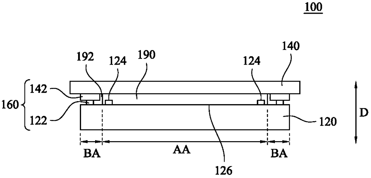
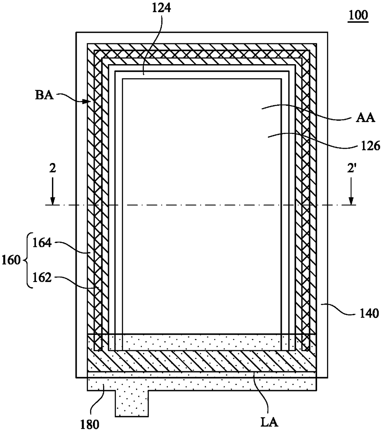
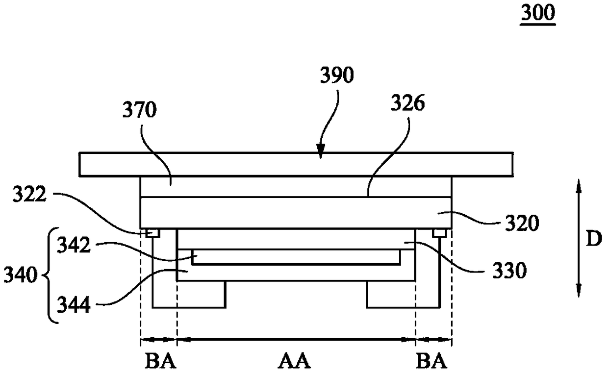
[0075] A number of embodiments of the present invention will be disclosed in the following figures. For the sake of clarity, many practical details will be described together in the following description. It should be understood, however, that these practical details should not be used to limit the invention. That is, in some embodiments of the present invention, these practical details are unnecessary. In addition, for the sake of simplifying the drawings, some well-known and commonly used structures and components are drawn in a simple and schematic manner in the drawings.

[0076] When a component is said to be "on", it can generally mean that the component is directly on top of other components, or that other components exist in between. Conversely, when a component is said to be "directly in" another component, it cannot have other components in between. As used herein, the word "and / or" includes any combination of one or more of the associated listed items.

[0077] ...


PUM


Abstract

The present invention relates to a touch display apparatus. The touch display apparatus comprises a touch sensing module, a protective layer and a static electricity protection assembly. The touch sensing module is provided with a sensing region and a peripheral region, wherein the peripheral region is adjacent to the sensing region. The protective layer is disposed opposite to the touch sensing module. The static electricity protection assembly is disposed between the touch sensing module and the protective layer and is located on vertical projection of the peripheral region in a stack direction of the touch sensing region and the protective layer. The static electricity protection assembly comprises a static electricity protection component and a metal loop element. The static electricity protection component is disposed on a surface, which faces the protective layer, of the touch sensing region. The metal loop element is disposed on a surface, which faces the touch sensing module, of the protective layer, and the protective layer is connected to the static electricity protection component by means of the metal loop element. Electrostatic charges accumulated on the protective layer can be rapidly transferred to the static electricity protection component by means of the metal loop element and are further transferred to a system for grounding, thereby reducing or avoiding influence of the electrostatic charges on a tough display device.

Description

technical field [0001] The present invention relates to a touch display device, in particular to a touch display device with an electrostatic charge discharge circuit. Background technique [0002] A common touch display device includes a protective layer, a touch sensing module, and a display module. In order to prevent electrostatic charge from accumulating in the touch display device, it will affect the electrical signal of the touch sensing module. Most of the touch sensing modules of touch display devices are provided with electrostatic discharge protection components located in non-touch sensing areas. It is true that installing an electrostatic protection component can quickly discharge part of the accumulated electrostatic charge, but because the material of the protective layer is usually made of plastic or glass in order to maintain light transmittance and protection functions, it is easy to be damaged by friction when the user touches the touch display device. Th...

Claims


Application Information

Patent Timeline
Patent Type & Authority Patents(China)
IPC IPC(8): G06F3/041
Inventor 姚立杰何姿谊陈彦华
Owner INTERFACE OPTOELECTRONICS SHENZHEN
Why Eureka
Try Eureka