Fingerprint sensor
A technology of fingerprint sensor and inductive switch, which is applied in the direction of instruments, character and pattern recognition, computer parts, etc., and can solve the problem of increasing
- Summary
- Abstract
- Description
- Claims
- Application Information
AI Technical Summary
Problems solved by technology
Method used
Image

Examples
Embodiment Construction
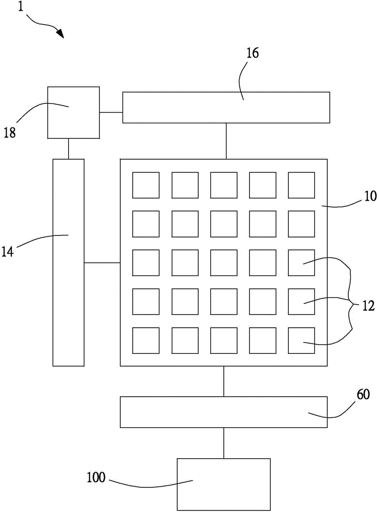
[0053] Please refer to figure 1 , which shows the component architecture of the fingerprint sensor 1 according to an embodiment of the present invention. The fingerprint sensor 1 includes a sensing insulating layer 10 , a plurality of sensing electrodes 12 , a row of multiplexers 14 , a column of multiplexers 16 , a controller 18 , and an offset elimination circuit 60 . Wherein, a plurality of sensing electrodes 12 are adjacent to the sensing insulating layer 10, and are electrically connected to the row multiplexer 14, the column multiplexer 16, and the offset elimination circuit 60, and the row multiplexer 14 is connected to the column multiplexer 16 is electrically connected with the controller 18. In more detail, each sensing electrode 12 is a pixel, a plurality of sensing electrodes 12 form a specific pixel array, and the specific pixel array has a specific number of rows and a specific number of columns, and the row multiplexer 14 The multiplexer 16 is based on a prese...
PUM
 Abstract
Description
Claims
Application Information