Ball grid array packaging structure

A ball grid array and packaging structure technology, which is applied in the direction of electrical components, electrical solid devices, circuits, etc., can solve the problems of additional cost of bottom glue, internal chip damage, cracking of the corners and edges of the packaging structure, etc.

Inactive Publication Date: 2007-07-04
POWERTECH TECHNOLOGY
View PDF0 Cites 8 Cited by
  • Summary
  • Abstract
  • Description
  • Claims
  • Application Information

AI Technical Summary

Problems solved by technology

However, when the BGA package structure is mounted to an external device by surface mount technology (SMT), it is easily squeezed by an external force 160, which will cause cracks around the corners of the package structure and damage to the internal chips.
The existing improved method is to fill the gap between the package structure and the printed circuit boar

Method used


Image

  • Ball grid array packaging structure
  • Ball grid array packaging structure
  • Ball grid array packaging structure

Examples


Embodiment Construction

[0016] A preferred embodiment is used below to illustrate the package structure of the ball grid array according to an embodiment of the present invention.

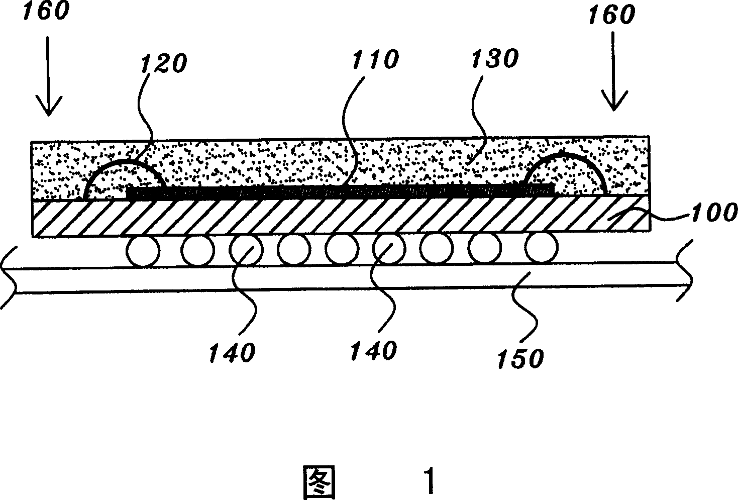
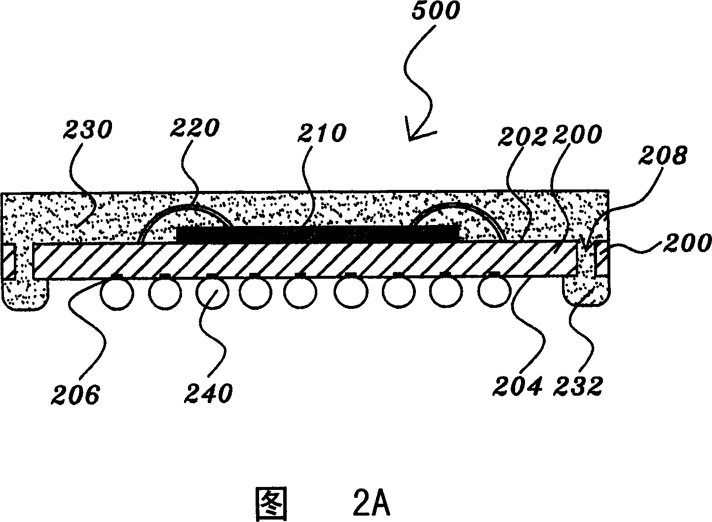
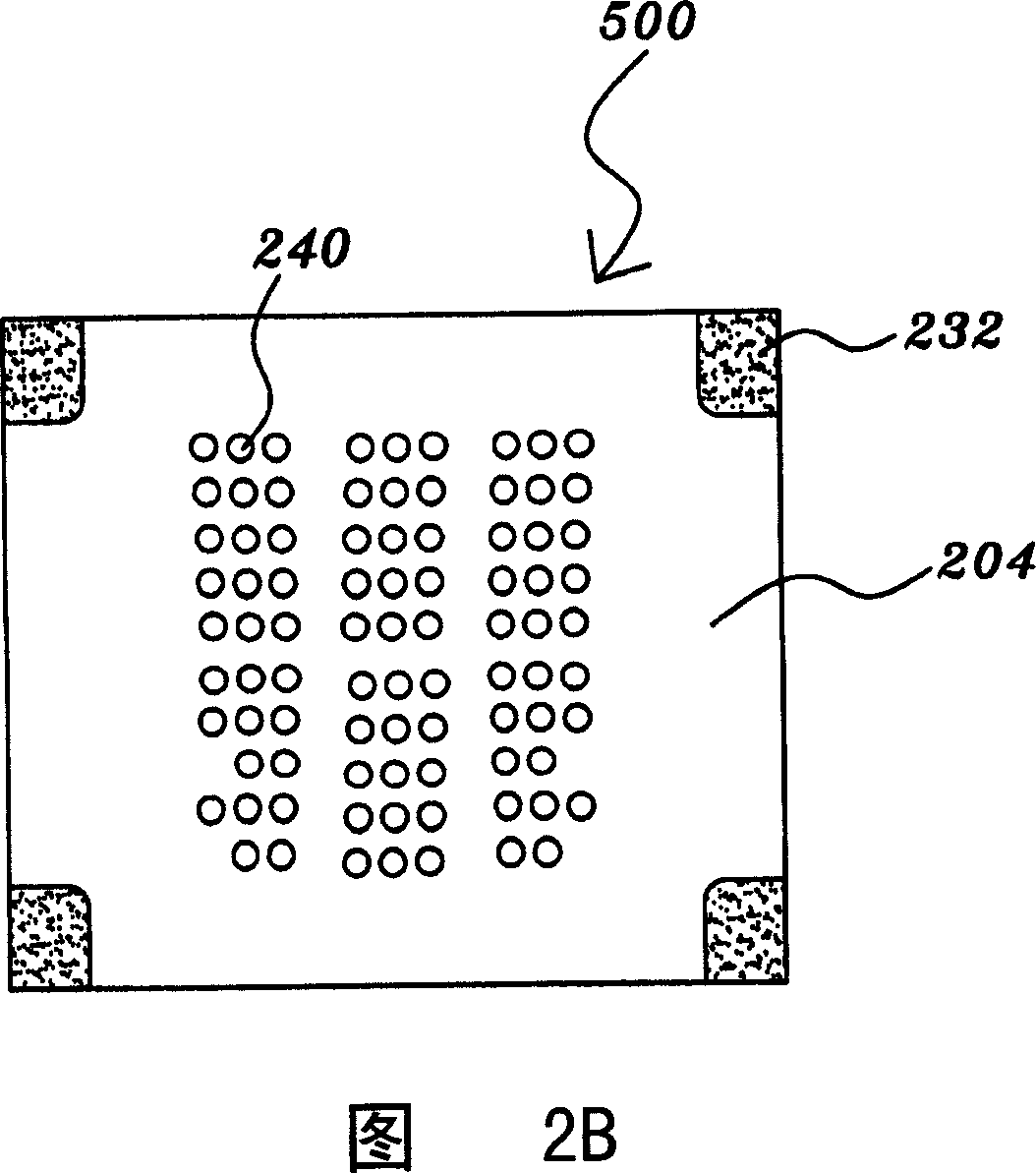
[0017] First, please refer to FIGS. 2A and 2B . FIG. 2A is a schematic cross-sectional view of a ball grid array package structure according to an embodiment of the present invention, and FIG. 2B is a schematic bottom view of the embodiment. As shown in the figure, in this embodiment, the ball grid array package structure 500 includes a substrate 200, for example, made of polyimide (polyimide), glass, aluminum oxide, beryllium oxide or elastomer (elastomer) material, The substrate 200 has an upper surface 202 and a lower surface 204 opposite to the upper surface 202, wherein the lower surface 204 is provided with a plurality of electrical contacts 206, and a chip 210 is arranged on the upper surface 202 of the substrate 200, and the chip 210 To electrically connect the above-mentioned plurality of electrical connection po...


PUM


Abstract

A ball grid array package structure, it sets multiple bumps in a ball grid array (BGA) substrate, and when making surface mount technology (SMT), it has more a supporting role to avoid the package structure bursting apart due to external force pressure, and also when the users use this semiconductor packaging module, the package structure can avoid damaging due to external force pressure.

Description

【Technical field】 [0001] The invention relates to a semiconductor packaging structure, in particular to a ball grid array packaging structure supported by a plurality of bumps. 【Background technique】 [0002] Press, the semiconductor packaging structure is an electronic device carrying active components such as semiconductor chips. The existing semiconductor packaging structure is such as a ball grid array packaging structure, as shown in Figure 1, which is a schematic cross-sectional view. This packaging structure is A chip 110 is arranged on a surface of a substrate 100, and then a wire bonding process is performed to form an electrical connection between the chip 110 and the substrate 100, and then an encapsulant 130 is used to coat the chip 110 and the bonding wire 120, and A plurality of solder balls 140 are planted in an array on the other surface of the substrate 100, and the solder balls 140 are used as input / output (I / O) terminals, so that the chip 110 mounted in th...

Claims


Application Information

Patent Timeline
IPC IPC(8): H01L23/31H01L23/488
CPCH01L2224/48091H01L2224/48227H01L2924/15311H01L2924/18301
Inventor 罗启彰
Owner POWERTECH TECHNOLOGY
Why Eureka
Try Eureka