Semiconductor storage device and programming method thereof

A technology of a storage device and a programming method, which is applied in the direction of information storage, static memory, read-only memory, etc., can solve problems such as priority reduction, and achieve the effect of reducing the time for data transmission and shortening the time for data programming

Active Publication Date: 2019-07-12
WINBOND ELECTRONICS CORP
View PDF7 Cites 0 Cited by
  • Summary
  • Abstract
  • Description
  • Claims
  • Application Information

AI Technical Summary

Problems solved by technology

Furthermore, Patent Document 3 discloses a flash memory in which ECC parity (Error Checking Correction parity) is added to input data to generate an ECC code, and the generated ECC code is written into a physical block, And when there is an error in the page (page) data read from the physical block, the error is corrected using the ECC code, and the physical block whose corrected error number is above the threshold is registered in the table as a warning block, and when the data is written Decreases the priority of selecting a warning block when

Method used


Image

  • Semiconductor storage device and programming method thereof
  • Semiconductor storage device and programming method thereof
  • Semiconductor storage device and programming method thereof

Examples


Embodiment Construction

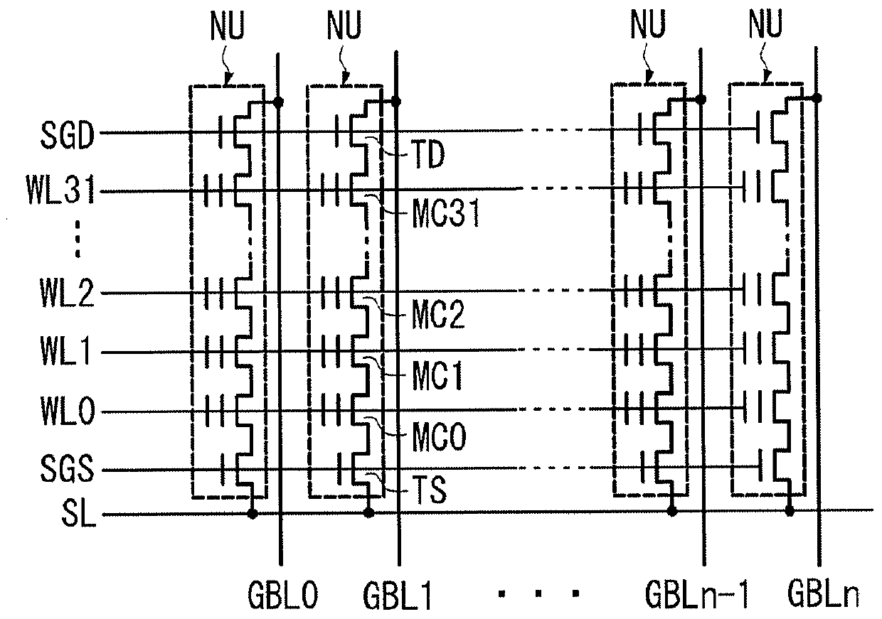
[0064] Next, embodiments of the present invention will be described in detail with reference to the drawings. Here, a NAND type flash memory is exemplified as an embodiment. In addition, it should be noted that each part is highlighted for ease of understanding in the drawings, but the scale of the actual device may not be the same.

[0065] 【Example】

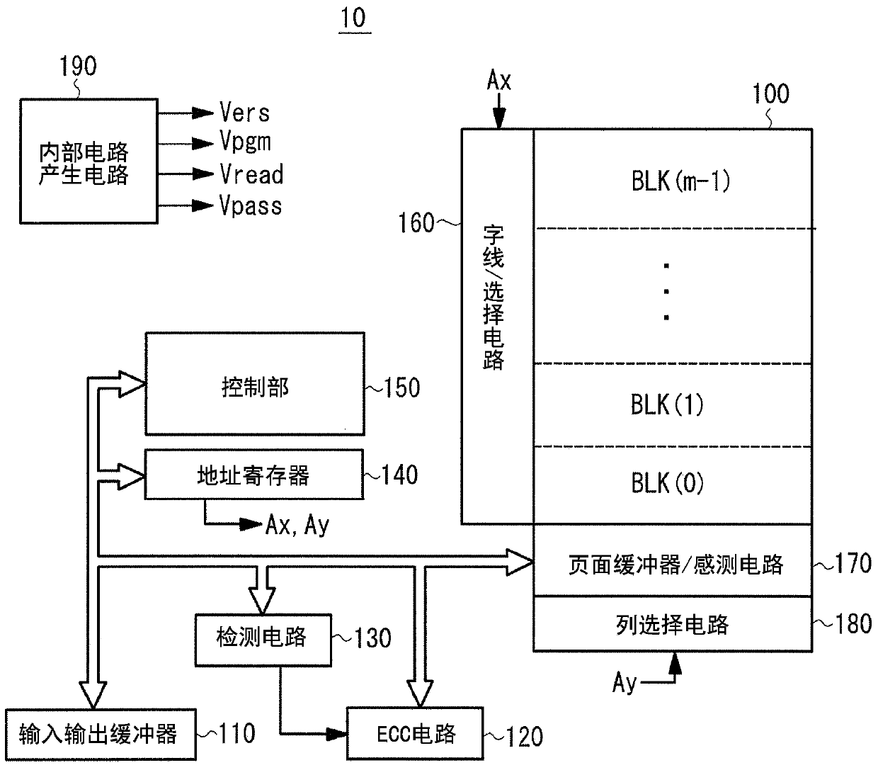
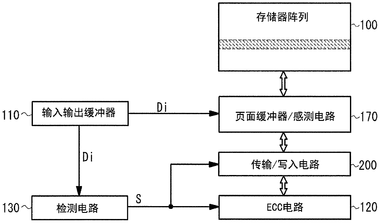
[0066] The typical composition of the flash memory of the embodiment of the present invention is shown in figure 1 . However, the configuration of the flash memory shown here is an example, and the present invention is not necessarily limited to this configuration. The flash memory 10 of the present embodiment is composed of: a memory array 100, a plurality of memory cells are arranged in a matrix; an input-output buffer 110 is connected to an external input-output terminal I / O, and maintains input-output data; an ECC circuit 120, performing error detection and correction on the data programmed in the memory array 100 or th...


PUM


Abstract

The invention provides a semiconductor memory device and a programming method thereof, which not only maintains reliability of data but also reduces programming time. A NAND-type flash memory loads programming data inputted from an external input / output terminal to a page buffer / sensing circuit. A detection circuit for monitoring the programming data detects whether the programming data is a special bit string, if the programming data is not the special bit string, a transmission / writing circuit transfers the programming data maintained in the page buffer / sensing circuit to an error detection correcting circuit and writes an error correcting code, which is generated through error detection correcting computation, to the page buffer / sensing circuit; and if the programming data is detected to be the special bit string, data transmission of the programming data maintained in the page buffer / sensing circuit is forbidden, and meanwhile, a known error correcting code being corresponding to the special bit string is written to the page buffer / sensing circuit.

Description

technical field [0001] The invention relates to a semiconductor storage device and a programming method thereof, to error detection and correction of input and output data of the semiconductor storage device, and in particular to an error detection and correction of input data of a NAND (NAND) type flash memory (Flash Memory). Correction. Background technique [0002] Semiconductor memories such as flash memory and Dynamic Random Access Memory (DRAM) are increasingly integrated year by year, making it difficult to manufacture memory elements without faults or defects. Therefore, on the memory chip, a redundancy scheme (redundancy scheme) for visually remedying the physical defect of the memory element generated in the manufacturing steps is adopted. For example, in a certain redundancy scheme, a physically defective storage element is remedied by setting a redundant memory. Furthermore, in the semiconductor memory, in addition to the physical recovery of the redundant memo...

Claims


Application Information

Patent Timeline
Patent Type & Authority Patents(China)
IPC IPC(8): G11C16/10G11C29/42
Inventor 山内一贵
Owner WINBOND ELECTRONICS CORP
Why Eureka
Try Eureka