Formation method of semiconductor device
A semiconductor and device technology, which is applied in the field of semiconductor device formation, can solve problems such as deformation stability and lower overall performance of semiconductor devices, and achieve the effect of improving stability and reducing differences
- Summary
- Abstract
- Description
- Claims
- Application Information
AI Technical Summary
Problems solved by technology
Method used
Image

Examples
Embodiment Construction
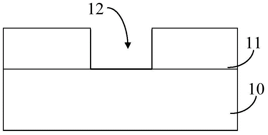
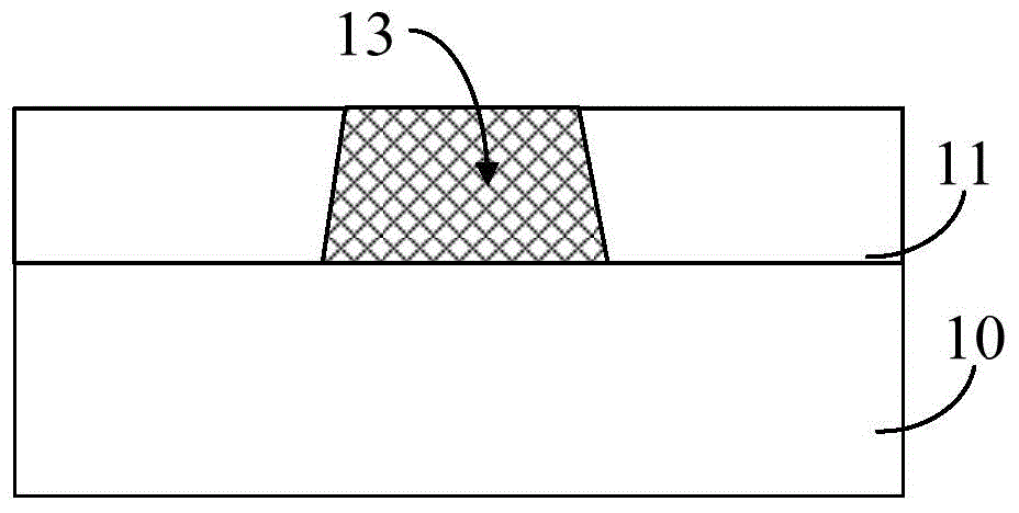
[0067] As mentioned in the background art, the metal gate formed by the back gate of the transistor in the prior art is prone to deformation, which leads to poor stability of the transistor.
[0068] combined reference figure 1 with figure 2 Analyzing the reason, after filling the gate opening 12 with the metal material, based on the characteristics of the metal material used to form the NMOS metal gate and the structure limitation of the gate opening, there are differences in the stress release of each part of the metal material in the metal gate, so that The formed metal material is deformed, so the finally formed NMOS metal gate structure is different from the original design structure (ie, the structure of the gate opening).
[0069] Specifically, such as figure 1 with figure 2 As shown, most of the originally designed metal gates are columnar structures with the width of the upper end and the width of the lower end being similar (i.e. the structure of the gate openin...
PUM
 Abstract
Description
Claims
Application Information
 - R&D
- Intellectual Property
- Life Sciences
- Materials
- Tech Scout
- Unparalleled Data Quality
- Higher Quality Content
- 60% Fewer Hallucinations
Browse by: Latest US Patents, China's latest patents, Technical Efficacy Thesaurus, Application Domain, Technology Topic, Popular Technical Reports.
© 2025 PatSnap. All rights reserved.Legal|Privacy policy|Modern Slavery Act Transparency Statement|Sitemap|About US| Contact US: help@patsnap.com