Liquid crystal display panel

A technology for liquid crystal display panels and display areas, which is applied in nonlinear optics, instruments, optics, etc., and can solve the problems that liquid crystal molecules cannot be fully filled, the yield and quality of the display panel 10 decrease, and the diffusion of liquid crystal molecules slows down, etc.

Active Publication Date: 2016-03-02
TCL CHINA STAR OPTOELECTRONICS TECH CO LTD
View PDF6 Cites 12 Cited by
  • Summary
  • Abstract
  • Description
  • Claims
  • Application Information

AI Technical Summary

Problems solved by technology

However, for a liquid crystal display panel 10 with a BOA substrate, the stacked thickness of the black matrix 15 in the display area AA is relatively thick, so that the depth D1 of the through hole H is relatively deep, and the diffusion of liquid crystal molecules is gradually slowed down, which is very easy to cause the display The liquid crystal molecules in the through hole H in the area AA cannot be filled, resulting in the generation of bubbles in the through hole H for 20
Compared with the non-display area BA, the non-display area BA does not have the stack of color photoresist layers 111, so the gap A2 of the liquid crystal layer 13 between the two substrates 11, 12 is relatively large, and the diffusion of liquid crystal molecules is relatively slow.
Moreover, the black matrix 15 in the non-display area BA also needs to be provided with a through hole H' designed for the connection of peripheral circuits. When the liquid crystal molecules diffuse to the non-display area BA, the gap A2 of the liquid crystal layer 13 between the two substrates 11 and 12 is relatively large, causing the liquid crystal molecules to The diffusion is slow, and the liquid crystal molecules cannot be fully filled into the through hole H', resulting in the generation of bubbles in the through hole H'20
[0005] In addition, the film thicknesses of the display area AA and the non-display area BA are different, resulting in large differences in the liquid crystal layer gaps A1 and A2 between the two, and it is also easy for the liquid crystal molecules in the display area AA and the non-display area BA to be unable to fully fill the through hole H. ,H', resulting in the generation of air bubbles 20 in the through hole H,H', and the air bubbles 20 will lead to a decline in the yield and quality of the liquid crystal display panel 10, affecting the display quality

Method used


Image

  • Liquid crystal display panel
  • Liquid crystal display panel

Examples


Embodiment Construction

[0019] Relevant technical content and detailed description of the present invention, now cooperate accompanying drawing to explain as follows:

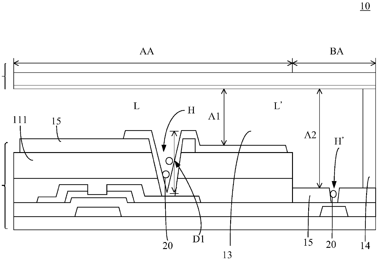
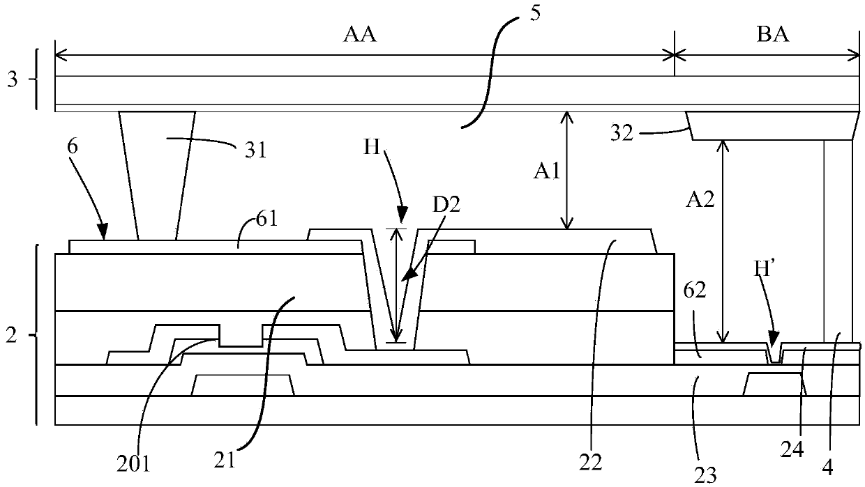
[0020] see figure 2 , which is a schematic structural diagram of a liquid crystal display panel in a preferred embodiment. The present invention provides a liquid crystal display panel 1, which belongs to a BOA (Blackmatrix on Array, BOA) type liquid crystal display panel, that is, the color photoresist layer and the black matrix are both Technology fabricated on thin film transistor array substrates. The liquid crystal display panel 1 includes: an array substrate 2 configured with a display area AA and a non-display area BA surrounding the display area AA; an opposing substrate 3 disposed above the array substrate 2; a sealant 4 disposed on the Between the array substrate 2 and the opposite substrate 3, the sealant ring 4 is wound around the non-display area BA; the liquid crystal layer 5 is arranged between the array substrate 2 a...


PUM

PropertyMeasurementUnit
thicknessaaaaaaaaaa

Abstract

The invention discloses a liquid crystal display panel comprising an array substrate, an opposite substrate, frame sealant, a liquid crystal layer, and a black matrix layer. The array substrate has a display area and a non-display area, and the display area includes multiple active components and a color photoresist layer. The opposite substrate is arranged above the array substrate. The frame sealant is arranged between the array substrate and the opposite substrate, and surrounds the non-display area. The liquid crystal layer is configured between the array substrate and the opposite substrate. The black matrix layer is arranged on the array substrate, and is distributed corresponding to the display area and the non-display area. The liquid crystal display panel is characterized in that at least the black matrix layer distributed in the non-display area has a thickness smaller than or equal to 2 microns. Thus, the thickness of the black matrix layer is reduced, the depth of the via on the array substrate is reduced, and bubbling in the via is prevented.

Description

technical field [0001] The invention relates to a liquid crystal display technology, in particular to a liquid crystal display panel which solves the problem of air bubbles around the liquid crystal panel. Background technique [0002] A traditional liquid crystal display panel is composed of a color filter substrate (ColorFilter Substrate), a thin film transistor array substrate (TFTArray Substrate), and a liquid crystal layer (Liquid Crystal Layer) arranged between the two substrates. Nowadays, the technology of making the color photoresist layer on the thin film transistor array substrate (ColorfilteronArray, COA) is proposed, and the technology of making the black matrix on the thin film transistor array substrate (BlackmatrixonArray, BOA) is further proposed, wherein BOA technology mainly assembles a BOA substrate with another opposing substrate, and fills the gap between the two substrates with liquid crystal molecules to form a liquid crystal layer, and solidifies the...

Claims


Application Information

Patent Timeline
Patent Type & Authority Applications(China)
IPC IPC(8): G02F1/1335
CPCG02F1/133512G02F1/133514
Inventor 叶成亮
Owner TCL CHINA STAR OPTOELECTRONICS TECH CO LTD
Why Eureka
Try Eureka