OLED device, OLED device manufacturing method and display

A technology of devices and device layers, applied in the field of OLED devices and their preparation methods and displays, can solve the problems of pixel shrinkage and impact on service life, and achieve the effects of solving pixel shrinkage, prolonging service life, and avoiding gas leakage

Active Publication Date: 2016-03-09
KUNSHAN GO VISIONOX OPTO ELECTRONICS CO LTD
View PDF5 Cites 7 Cited by
  • Summary
  • Abstract
  • Description
  • Claims
  • Application Information

AI Technical Summary

Problems solved by technology

[0003] Based on this, it is necessary to provide an OLED device and its preparation method and display f

Method used


Image

  • OLED device, OLED device manufacturing method and display
  • OLED device, OLED device manufacturing method and display
  • OLED device, OLED device manufacturing method and display

Examples


Embodiment Construction

[0029] In order to make the technical solution of the present invention clearer, the following further describes the present invention in detail with reference to the accompanying drawings and specific embodiments.

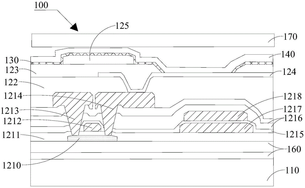
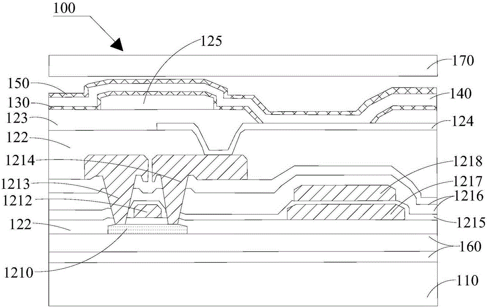
[0030] First, it should be noted that the functional layer refers to a TFT (Thin Film Transistor, thin film transistor) layer formed on a substrate. It can specifically include a gate, a source, a drain, and an active layer. It may also include a planarization layer, a pixel defining layer, and support pillars or isolation pillars.

[0031] The OLED device layer specifically includes a first organic layer and a cathode sequentially formed on the first water-absorbing layer. Generally, it may also include a second organic layer formed on the cathode.

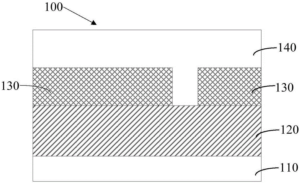
[0032] Among them, see figure 1 As a specific embodiment of the OLED device 100 of the present invention, that is, the first embodiment, it includes a substrate 110, a functional layer 120 formed on the substrate 110, and...


PUM

PropertyMeasurementUnit
Thicknessaaaaaaaaaa
Thicknessaaaaaaaaaa

Abstract

The invention discloses an OLED device, an OLED device manufacturing method and a display. The OLED device comprises a substrate, a functional layer, a first water absorption layer and an OLED device layer, wherein the functional layer is formed on the substrate; the first water absorption layer is formed on the functional layer and covers the functional layer except a light-emitting region; and the OLED device layer is formed on the first water absorption layer and the functional layer which is not covered by the first water absorption layer. According to the invention, the first water absorption layer is added between the functional layer and the OLED device layer of the OLED device, thus, the situation of out gassing generated in follow-up evaporation of organic materials and caused by water vapor or sol residuals generated in earlier-stage production technological process is avoided effectively. Finally, a problem of influence on service life of the conventional OLED device caused by a phenomenon of pixel shrinkage of the conventional OLED device caused by non-packaging problems is solved effectively.

Description

Technical field [0001] The invention relates to the field of organic light-emitting displays, in particular to an OLED device, a preparation method thereof, and a display. Background technique [0002] At present, organic glue is used in the production process of OLED (Organic Light-Emitting, also known as organic electric laser display). Such as: PMOLED (PassivematrixOLED, passive organic light-emitting diode) and AMOLED (Active-Matrix Organic Light-Emitting, active-matrix organic light-emitting diode, also known as active organic light-emitting display) in the preparation of functional layers such as pixel defining layer and isolation column. Among them, LTPS (Low Temperature Poly-silicon) substrates are mostly used as TFT (thin film transistor) substrates in AMOLED. However, in the production process of the LTPS substrate, an organic glue is usually required to prepare the planarization layer, the pixel defining layer, and the isolation column or support column in the functio...

Claims


Application Information

Patent Timeline
IPC IPC(8): H01L51/50H01L51/52H01L51/56H01L27/32
CPCH10K59/00H10K50/00H10K50/80H10K50/846H10K71/00
Inventor 向桂华甘帅燕朱修剑
Owner KUNSHAN GO VISIONOX OPTO ELECTRONICS CO LTD
Why Eureka
Try Eureka