Printed board connecting structure
A technology of printed circuit board and connection structure, which is applied in the direction of circuits, connections, parts of connection devices, etc., which can solve the problems of printed circuit boards not being connected correctly, difficult to plug in and out of connectors, and damage to connectors, etc., to achieve simple Guidance function, easy plug-in effect
- Summary
- Abstract
- Description
- Claims
- Application Information
AI Technical Summary
Problems solved by technology
Method used
Image

Examples
Embodiment approach 1
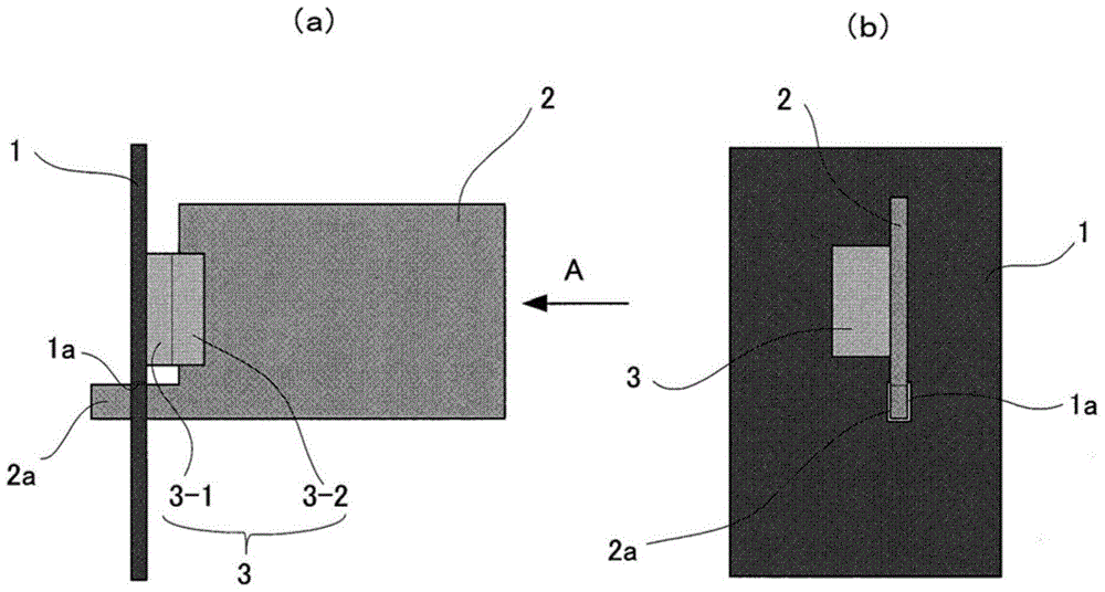
[0033] figure 1 It is a figure which shows the key part of 1st Embodiment (Embodiment 1) of the connection structure of the printed circuit board concerning this invention, figure 1 (a) is a side view, figure 1 (b) is viewed from the direction of arrow A figure 1 The diagram of (a).
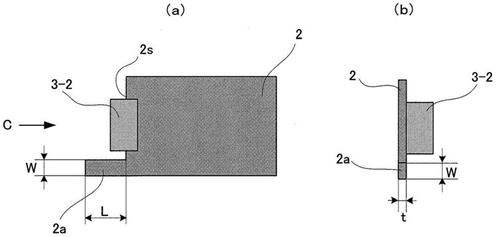
[0034] exist figure 1 Among them, 1 is the first printed circuit board (main board), 2 is the second printed circuit board (sub-board), and 3 is the connector (male and female connector) connecting the main board 1 and sub-board 2, using a cheap Connector as connector 3.
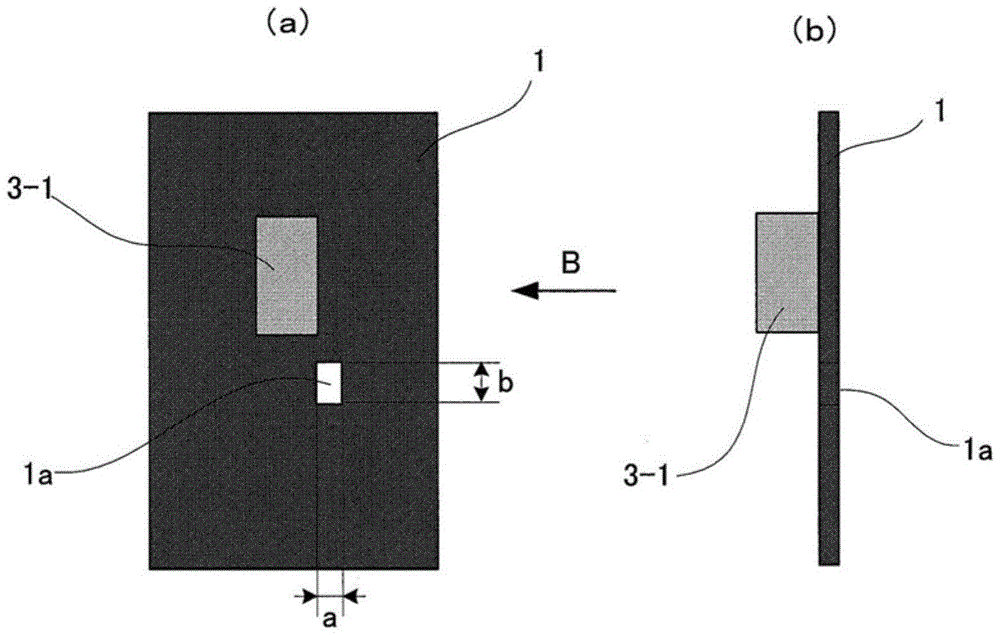
[0035] Such as figure 2 The top view of the motherboard 1 of (a), figure 2 The side view of the motherboard 1 of (b) (observed from the arrow B direction figure 2 As shown in the figure (a) of (a), one of the male and female connectors 3 is mounted on the motherboard 1 as the first connector 3-1, and a guiding guide is formed on the peripheral substrate surface of the first connector 3-1. hole 1a.
[0036] Also, if ...
Embodiment approach 2
[0043] Figure 5 (a) is a figure which shows the key part of 2nd Embodiment (Embodiment 2) of the connection structure of the printed circuit board which concerns on this invention, Figure 5 (a) is a side view, Figure 5 (b) is viewed from the direction of arrow A Figure 5 The diagram of (a).
[0044] exist Figure 5 Among them, 1 is the first printed circuit board (main board), 2A and 2B are the second printed circuit boards (sub-boards), 3A and 3B are connectors (female and female connectors) connecting the main board 1 and sub-boards 2A and 2B, which are not used The same type of inexpensive connectors having a guiding function are used as the connectors 3A, 3B.
[0045] Such as Image 6 The top view of the motherboard 1 of (a), Image 6 The side view of the motherboard 1 of (b) (observed from the arrow B direction Image 6 As shown in (a)), the motherboard 1 is provided with a first sub-board mounting portion 1A and a second sub-board mounting portion 1B.
[0046...
Embodiment approach 3
[0063] Figure 11 (a) is a figure which shows the key part of the 3rd embodiment (Embodiment 3) of the connection structure of the printed circuit board which concerns on this invention, Figure 11 (a) is a side view, Figure 11 (b) is viewed from the direction of arrow A Figure 11 The diagram of (a).
[0064] If the connection structure of the printed circuit board of the third embodiment is adopted, the connection structure of the printed circuit board of the first embodiment ( figure 1 ), a conductive pattern PT1 (PT1 1 ~PT1 4 ) (see Figure 12 ). Also, a conductive pattern PT2 (PT2) is formed around the protrusion 2a for guiding the sub-board 2. 1 ~PT2 4 ) (see Figure 13 ).
[0065] in addition, Figure 12 (a) is a top view of the main board 1, Figure 12 (b) is an enlarged view around the guide hole 1 a of the main board 1 . Conductive pattern PT1 1 ~PT1 4 Four places around the guide hole 1 a are formed extending from the inner wall surface of the hole 1...
PUM
 Abstract
Description
Claims
Application Information
 - Generate Ideas
- Intellectual Property
- Life Sciences
- Materials
- Tech Scout
- Unparalleled Data Quality
- Higher Quality Content
- 60% Fewer Hallucinations
Browse by: Latest US Patents, China's latest patents, Technical Efficacy Thesaurus, Application Domain, Technology Topic, Popular Technical Reports.
© 2025 PatSnap. All rights reserved.Legal|Privacy policy|Modern Slavery Act Transparency Statement|Sitemap|About US| Contact US: help@patsnap.com