Supercharge Your Innovation With Domain-Expert AI Agents!

A new oled electron transport material and its application

An electron transport material, a new type of technology, applied in the field of photoelectrochemistry, can solve the problems of high driving voltage, low luminous brightness and efficiency, without attracting too much attention, and achieve lower driving voltage, high electron transport performance, and long practical life Effect

Active Publication Date: 2017-10-10
VALIANT CO LTD
View PDF1 Cites 0 Cited by
  • Summary
  • Abstract
  • Description
  • Claims
  • Application Information

AI Technical Summary

Problems solved by technology

[0002] The origin of organic electroluminescent devices (OLEDs) can be traced back to the 1960s. Pope et al. applied DC voltage to anthracene single crystals to make them emit light. However, due to the high driving voltage (100V) and relatively high brightness and efficiency low, did not attract much attention

Method used


Image

  • A new oled electron transport material and its application
  • A new oled electron transport material and its application
  • A new oled electron transport material and its application

Examples


preparation Embodiment 1

[0041] Preparation Example 1 Preparation of Compound 1-1

[0042]

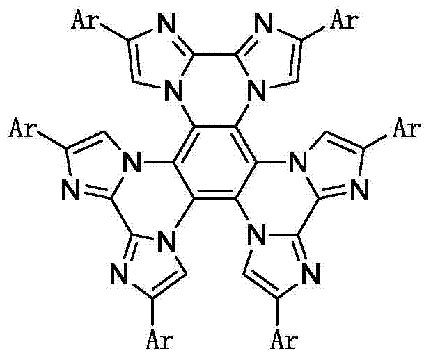
[0043] Add 3.3g (0.01mol) of 2,3,6,7,10,11-hexaamino-1,4,5,8,9,12-hexaazatriethylene obtained in the above preparation example to a 500mL three-necked flask in sequence Benzene, 20g (0.1mol) α-bromoacetophenone, 16.8g sodium bicarbonate, 300g DMF (N,N-dimethylformamide), 120 ℃ heat preservation reaction for 12h, the reaction solution was poured into 500g water, the system A large amount of yellow powder was precipitated, filtered by suction, and the filter cake was rinsed with 100 g of acetone and 100 g of absolute ethanol in sequence, and then vacuum-dried at 80° C. for 12 hours to prepare 3.2 g of yellow powder with a yield of 34.6%.

[0044] Weigh 3g of yellow powder, put it in a vacuum sublimation apparatus (Shenyang Huiyu, ZDF-52278), the sublimation parameter is that the sublimation vacuum is 2×10 -5 Pa, the temperature of the sublimation zone 3 is 360°C, the temperature of the sublimation zone 2 is ...

preparation Embodiment 2

[0045] Synthesis of Preparation Example Two Compound 1-2

[0046] Compound 1-2 reacts with intermediate 2,3,6,7,10,11-hexaamino-1,4,5,8,9,12-hexaazatriphenylene using α-bromo-1-naphthylethanone It is prepared with a yield of 85%, a high-resolution mass spectrum theoretical value of 1225.4125, and a test value of 1225.4120.

preparation Embodiment 3

[0047] Synthesis of Preparation Example Three Compound 1-3

[0048] Reaction of compound 1-3 with intermediate 2,3,6,7,10,11-hexaamino-1,4,5,8,9,12-hexaazatriphenylene using α-bromo-2-naphthylethanone It is prepared with a yield of 85%, a high-resolution mass spectrum theoretical value of 1225.4125, and a test value of 1225.4120.


PUM


Abstract

The present invention relates to a novel OLED electron transport material and its application. The novel OLED electron transport material has the general structural formula shown below, wherein Ar is an aromatic group. The novel OLED electron transport material provided by the invention has stable properties and high carrier mobility, and can be used in the electron transport layer of OLED devices. The applied OLED devices can significantly reduce the driving voltage and improve the current efficiency.

Description

technical field [0001] The invention relates to a novel OLED electron transport material and its application, belonging to the field of photoelectrochemistry. Background technique [0002] The origin of organic electroluminescent devices (OLEDs) can be traced back to the 1960s. Pope et al. applied DC voltage to anthracene single crystals to make them emit light. However, due to the high driving voltage (100V) and relatively high brightness and efficiency low, without much attention. With the continuous improvement of technology. In 1987, C.W.Tang et al. of Kodak Company used 8-hydroxyquinoline aluminum (AIq 3 ) is a light-emitting material, and a double-layer sandwich structure OLED device is made by vacuum evaporation method. The turn-on voltage is only a few volts, and the brightness can reach up to 1000cd / m 2 , marking OLED has taken an important step towards practical application and has become an important milestone in the field of organic electroluminescence. [000...

Claims


Application Information

Patent Timeline
Patent Type & Authority Patents(China)
IPC IPC(8): C07D487/22H01L51/54
CPCC07D487/22H10K85/6572
Inventor 刘英瑞石宇林存生高自良杨腾李韶涛
Owner VALIANT CO LTD
Features
  • R&D
  • Intellectual Property
  • Life Sciences
  • Materials
  • Tech Scout
  • Unparalleled Data Quality
  • Higher Quality Content
  • 60% Fewer Hallucinations
Learn More