Display screen with mirror function, control method, device and terminal
A display screen and functional technology, applied in the direction of static indicators, instruments, telephone structures, etc., can solve the problems of affecting transmission and low reflectivity
- Summary
- Abstract
- Description
- Claims
- Application Information
AI Technical Summary
Problems solved by technology
Method used
Image
Examples
Embodiment 1
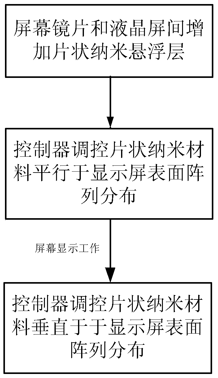
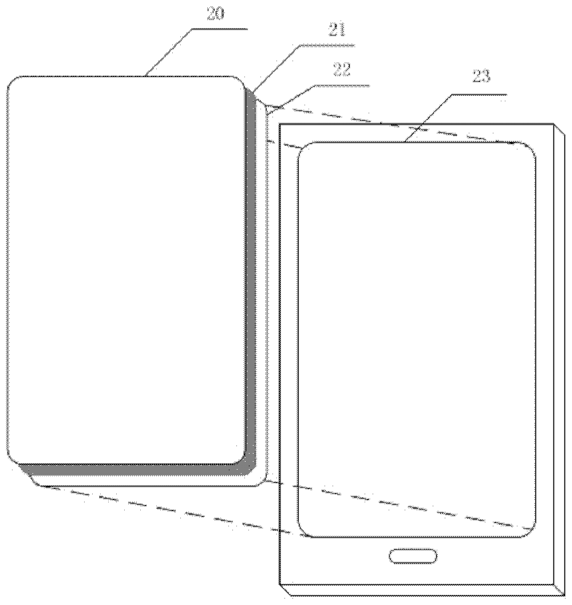
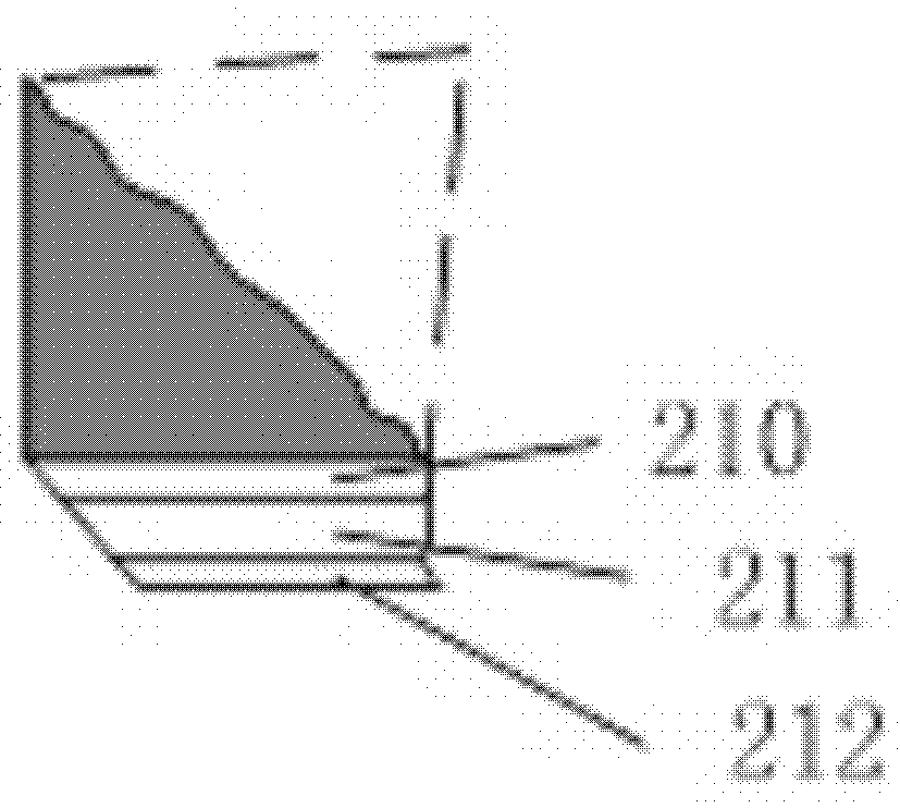
[0050] Such as figure 1 and 2 As shown, between the screen lens 20 and the liquid crystal screen 22, a sheet-like nanomaterial suspension layer 21 is sandwiched. Specifically, a graphene sheet (between 1um and 10um in size) coated with 10nm thick silver on both sides is used here as a sheet-shaped nanomaterial, and an aqueous solvent of SDS (sodium dodecyl sulfate, a dispersion liquid) is dissolved. , SDS is to avoid the aggregation of graphene sheets. When realizing the function of the mirror surface, the bottom magnetic layer 23 provides a static magnetic field perpendicular to the surface. Under the action of this static magnetic field, the graphene sheets are arranged perpendicular to the magnetic field due to their diamagnetic properties, and are distributed horizontally parallel to the surface of the display screen, forming a reflective surface. Such as image 3A partial enlarged view of the flaky nanomaterial suspension layer 21, the nanomaterial suspension 211 is c...
Embodiment 2
[0052] Such as figure 1 and 2 As shown, the bottom magnetic layer 23 always exists in this embodiment, and the default state of the flake nanomaterial suspension layer 21 is a mirror. Like this, when mobile phone black screen, even shut off power supply, screen can be one side silver reflecting mirror, and when display screen is woken up, and voltage is applied to the upper pole plate 210 of flake nanomaterial suspension layer 21, and screen can transmit light normally again.
[0053] At this time, the need to switch outfields can be reduced. Since the influence of the electric field can be much greater than that of the magnetic field, the torsional moment ratio can exceed 10 4 , so when the terminal screen shows light transmission, the effect of the magnetic field is almost completely offset, and the flake nanomaterial can form an array distribution with good uprightness. In this embodiment, the thickness of the flake nanomaterial is about 20nm, and its surface size is 1um ...
PUM
| Property | Measurement | Unit |
|---|---|---|
| thickness | aaaaa | aaaaa |
| thickness | aaaaa | aaaaa |
Abstract
Description
Claims
Application Information


