Method of forming semiconductor structure

A semiconductor and fin technology, which is applied in the field of semiconductor structure formation, can solve the problems of bad influence of semiconductor structure performance, difficult control of doping ion channel effect, etc., so as to suppress diffusion and channel effect, improve channel effect, and improve performance effect

Active Publication Date: 2016-03-30
SEMICON MFG INT (SHANGHAI) CORP
View PDF2 Cites 2 Cited by
  • Summary
  • Abstract
  • Description
  • Claims
  • Application Information

AI Technical Summary

Problems solved by technology

[0005] However, in the above-mentioned high-temperature ion implantation process, it is difficult to control the diffusion of dopant ions and the channeling effect during the implantation process, which will adversely affect the performance of the final semiconductor structure.

Method used


Image

  • Method of forming semiconductor structure
  • Method of forming semiconductor structure
  • Method of forming semiconductor structure

Examples


Embodiment Construction

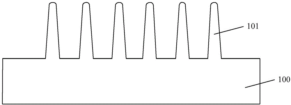
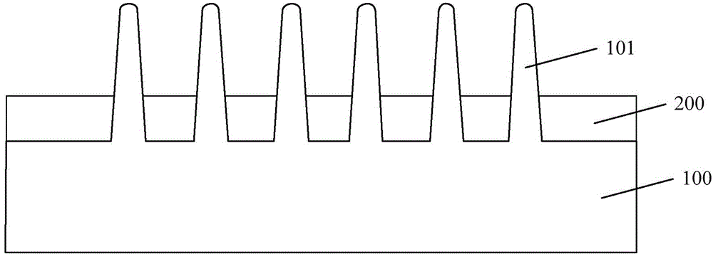
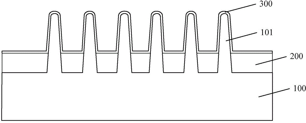
[0028] As mentioned in the background art, although high-temperature ion implantation can reduce implant damage in the current ion implantation process, it will aggravate implanted ion diffusion and channeling effects, which will affect the performance of the final formed semiconductor structure.

[0029] Research has found that during the high-temperature ion implantation process, the temperature of the substrate to be implanted is high, and the implanted ions have a high diffusion rate at high temperature, and it is easier to diffuse outside the implanted area, making it difficult to control the position of the implanted area , forming a shallow knot. Moreover, since the implantation damage of high-temperature ion implantation is small, no amorphous layer will be formed on the surface of the substrate, and the surface of the implanted substrate still has a relatively complete lattice structure, and channeling is easy to occur during the implantation process, making the implan...


PUM

PropertyMeasurementUnit
Thicknessaaaaaaaaaa

Abstract

A method of forming a semiconductor structure comprises the steps of providing a semiconductor substrate, the surface of which is provided with a plurality of separate fin portions; forming an isolation layer on the surface of the semiconductor substrate, the surface of the isolation being lower than top surfaces of the fin portions and partially covering side walls of the fin portions; forming an diffusion preventing layer on the surfaces of the fin portions; then, carrying out diffusion preventing ion implantation for the fin portions; and afterwards, carrying out N-type or P-type doped ion implantation for the fin portions. The method can improve the performance of the formed semiconductor structure.

Description

technical field [0001] The invention relates to the technical field of semiconductors, in particular to a method for forming a semiconductor structure. Background technique [0002] The ion implantation process is a very commonly used ion doping process in semiconductor technology, which is used to dope various ions in the semiconductor substrate. In the formation process of transistors, ion implantation process can be used to form a well region in the semiconductor substrate, ion implantation can be used to adjust the threshold voltage of the transistor to be formed, and lightly doped ion implantation and heavily doped ion implantation can be used to form the source of the transistor. pole and drain. [0003] The ion implantation process injects charged and energetic particles into the substrate, and high-energy ions lose energy due to collisions with electrons and nuclei in the substrate, and stay at a certain depth in the crystal lattice. Since the implanted ions have c...

Claims


Application Information

Patent Timeline
IPC IPC(8): H01L21/336
Inventor 谢欣云
Owner SEMICON MFG INT (SHANGHAI) CORP
Why Eureka
Try Eureka