Supercharge Your Innovation With Domain-Expert AI Agents!

Array base plate and preparing method thereof, display device

A technology of an array substrate and a manufacturing method, which is applied in the display field, can solve problems such as poor electrical process, and achieve the effect of avoiding poor electrical process of TFT

Inactive Publication Date: 2016-03-30
BOE TECH GRP CO LTD +1
View PDF6 Cites 6 Cited by
  • Summary
  • Abstract
  • Description
  • Claims
  • Application Information

AI Technical Summary

Problems solved by technology

[0004] Embodiments of the present invention provide an array substrate, a manufacturing method thereof, and a display device, which are used to solve the problem in the prior art that the TFT electrical process is poor due to the contact between the residue of the active layer and the conductive layer.

Method used


Image

  • Array base plate and preparing method thereof, display device
  • Array base plate and preparing method thereof, display device
  • Array base plate and preparing method thereof, display device

Examples


Embodiment Construction

[0052] In order to make the objectives, technical solutions and advantages of the present invention clearer, the present invention will be further described in detail below with reference to the accompanying drawings. Obviously, the described embodiments are only a part of the embodiments of the present invention, not all of the embodiments. Based on the embodiments of the present invention, all other embodiments obtained by those of ordinary skill in the art without creative efforts shall fall within the protection scope of the present invention.

[0053] The technical solutions involved in the present invention are described in detail below through specific embodiments, and the present invention includes but is not limited to the following embodiments.

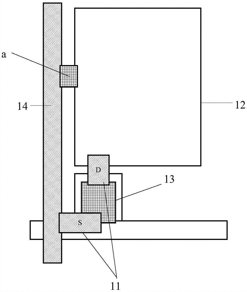
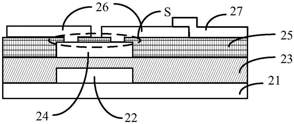
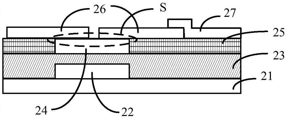
[0054]The present invention provides an array substrate, the array substrate mainly includes: a gate insulating layer, an active layer, a source and drain electrodes in contact with the active layer, and a first conductive la...


PUM


Abstract

The invention discloses an array base plate and a preparing method thereof, and a display device. The main content comprises that a grid insulating layer is arranged on one surface of an active layer; an isolation insulating layer is arranged on the other surface; therefore the active layer and the adjacent other first conductive layer are isolated well; further the residue of the active layer is prevented from overlapping any first conductive layer; especially the condition that the residue of the active layer overlaps a pixel electrode and a data wire is effectively avoided; therefore the TFT electricity badness problem resulted from overlapping is solved; simultaneously the isolation insulating layer is added, the thickness of the film layer can be adjusted suitably; therefore the height difference of the film layer surface of the whole array base plate after the film layer forms the active layer is reduced; the smoothness of the film layer surface is improved; the subsequent film layer can deposit better under the condition that the gradient angle of the film layer surface is relatively small; the phenomenon of film layer rupture resulted from relatively high height difference or relatively large gradient angle of the film layer surface is reduced.

Description

technical field [0001] The present invention relates to the field of display technology, and in particular, to an array substrate, a manufacturing method thereof, and a display device. Background technique [0002] In the prior art, the preparation process of the active layer (semiconductor layer) can simultaneously deposit SiN x , a-Si, N+a-Si, and then perform a patterning process on the deposited mixed film layer to form a patterned active layer. [0003] However, in the specific preparation process, due to the preparation environment, equipment or other abnormal reasons, it is inevitable that foreign objects such as dust and debris will adhere to the mixed film layer. These foreign objects can be attached during the deposition process. process or attach while etching. During the dry etching process, due to the presence of foreign objects in some positions of the mixed film layer, the gas used for dry etching cannot contact and react with the film layer, resulting in re...

Claims


Application Information

Patent Timeline
Patent Type & Authority Applications(China)
IPC IPC(8): H01L27/12H01L21/77
CPCH01L27/1214H01L27/1244H01L27/1259G02F1/1368H01L29/78636H01L27/1248G02F1/1343G02F1/136227G02F1/136277G02F1/136286G02F2201/123H01L27/124H01L27/1262
Inventor 林子锦赵海生彭志龙孙东江
Owner BOE TECH GRP CO LTD
Features
  • R&D
  • Intellectual Property
  • Life Sciences
  • Materials
  • Tech Scout
  • Unparalleled Data Quality
  • Higher Quality Content
  • 60% Fewer Hallucinations
Learn More