A screen packaging cover, screen body and screen packaging and cutting method
A cutting method and packaging cover technology, which is applied in the manufacture of electric solid devices, semiconductor devices, semiconductor/solid devices, etc., can solve problems such as limited application range, broken lead wire failure, and lead wire damage on the surface of the substrate, so as to improve cutting efficiency Effect
- Summary
- Abstract
- Description
- Claims
- Application Information
AI Technical Summary
Problems solved by technology
Method used
Image

Examples
Embodiment 1
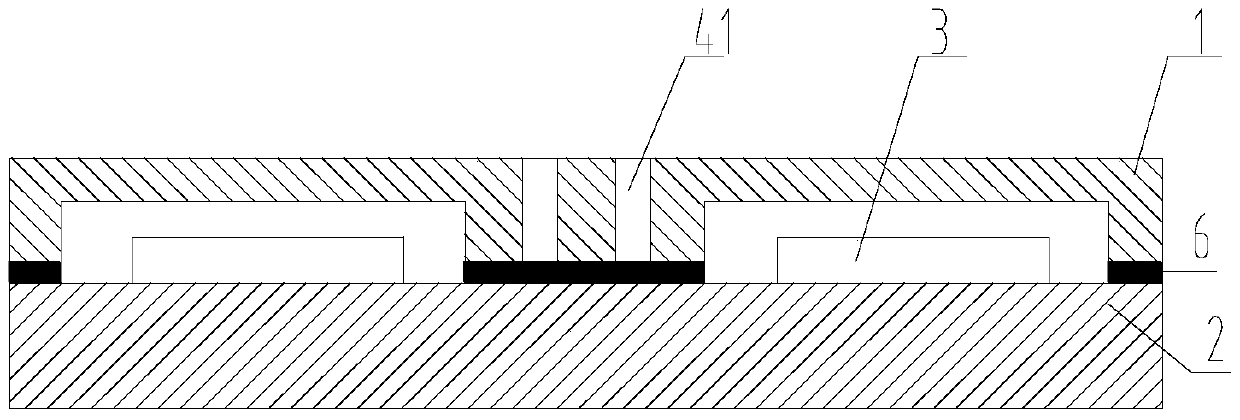
[0037] Such as figure 1 with Figure 4 As shown, the manufacturing method of the reserved lead-out positions on the package cover specifically includes: digging corresponding through holes 41 in the package cover corresponding to the lead area of the organic light emitting unit in advance, and then bonding the substrate 2 and the package cover; The cutting tool cuts the screen body along the cutting line 5 of the peripheral frame of the through hole, and the lead area of the organic light emitting unit 3 is led out through the through hole 41 to facilitate driving the FPC pressing.
Embodiment 2
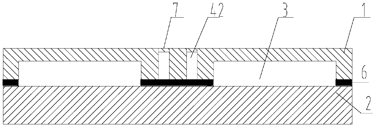
[0039] Such as figure 2 with Figure 5 As shown, the manufacturing method of the reserved lead-out position on the package cover specifically includes: digging corresponding hollow through holes 42 in the package cover corresponding to the lead area of the organic light-emitting unit in advance, and then bonding the substrate and the package cover; The cutting tool cuts the screen body along the peripheral frame of the hollow cut line; the split area 7 of the hollow through hole 42 can be removed to form a through hole, and the lead area of the organic light emitting unit 3 is led out through the through hole to facilitate driving FPC pressing.
Embodiment 3
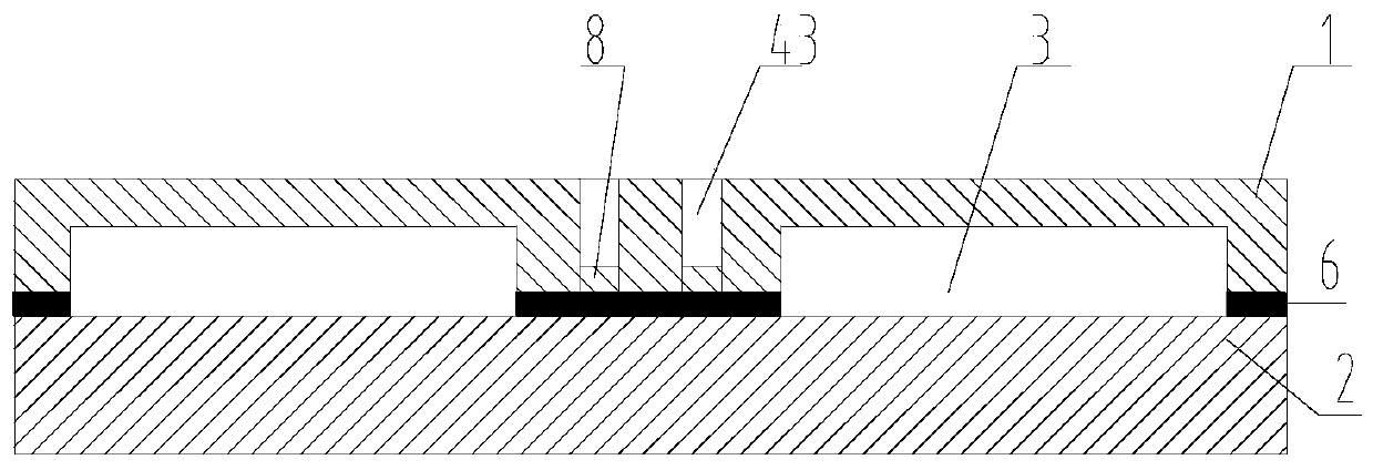
[0041] Such as image 3 with Image 6 As shown, the manufacturing method of the reserved lead-out position specifically includes: pre-cutting a pre-cut groove on the package cover corresponding to the lead area of the organic light-emitting unit, and the cutting depth is 1 / 2-9 / 10 of the package cover thickness , And then bond the substrate and the package cover; cut the screen with a cutting tool along the outer frame of the pre-cut line; after the substrate is cut, the package cover part is broken off along the pre-cut line and the pre-cut groove is removed In the split 8, the lead area of the organic light-emitting unit is led out through the pre-cut groove 43.
[0042] The sequence numbers of the foregoing embodiments of the present invention are only for description, and do not represent the superiority of the embodiments.
[0043] The above descriptions are only preferred embodiments of the present invention and are not intended to limit the present invention. Any modifica...
PUM
 Abstract
Description
Claims
Application Information
 - R&D
- Intellectual Property
- Life Sciences
- Materials
- Tech Scout
- Unparalleled Data Quality
- Higher Quality Content
- 60% Fewer Hallucinations
Browse by: Latest US Patents, China's latest patents, Technical Efficacy Thesaurus, Application Domain, Technology Topic, Popular Technical Reports.
© 2025 PatSnap. All rights reserved.Legal|Privacy policy|Modern Slavery Act Transparency Statement|Sitemap|About US| Contact US: help@patsnap.com