Brightness deviation compensation apparatus and compensation method of display device

A technology for compensating equipment and light-emitting displays, applied in static indicators, instruments, etc., can solve the problems of complicated steps, reduced brightness, and cumbersomeness, and achieve the effects of simplifying circuit configuration, reducing aperture ratio, and shortening time.

Inactive Publication Date: 2016-03-30
NEOVIEWKOLON
View PDF10 Cites 19 Cited by
  • Summary
  • Abstract
  • Description
  • Claims
  • Application Information

AI Technical Summary

Problems solved by technology

Therefore, there is a problem that the steps of measuring the change in characteristics due to the use of the display are complicated and cumbersome, and it takes a lot of time to measure the change in characteristics
[0025] In addition, Patent Document 2 does not consider performance degradation of the driving transistor, which is one of the causes of degradation in characteristics due to use of the display, and thus does not completely solve the problem of performance degradation due to long-term use of the display
[0026] In addition, it is necessary to separately provide a voltage sensing circuit including a transistor, which senses a voltage of one surface of the organic electroluminescent device to generate a feedback signal, which leads to a problem that the aperture ratio of the display is lowered and the brightness is lowered.

Method used


Image

  • Brightness deviation compensation apparatus and compensation method of display device
  • Brightness deviation compensation apparatus and compensation method of display device
  • Brightness deviation compensation apparatus and compensation method of display device

Examples


Embodiment 1

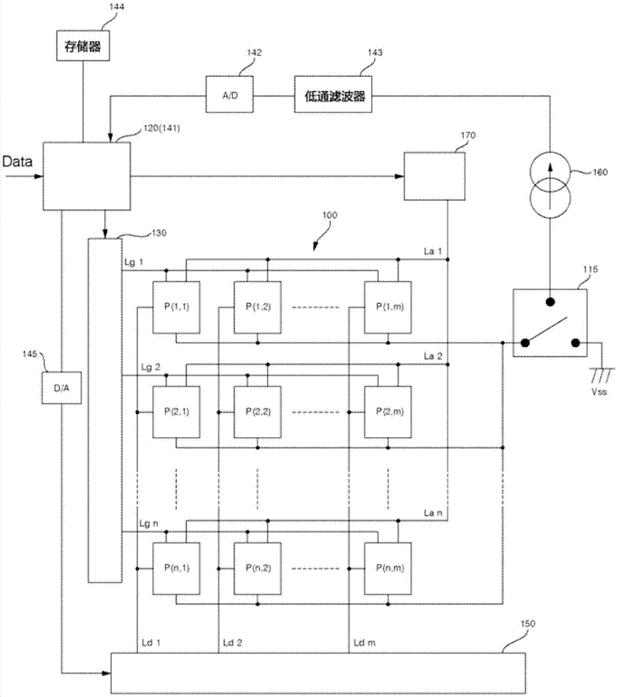
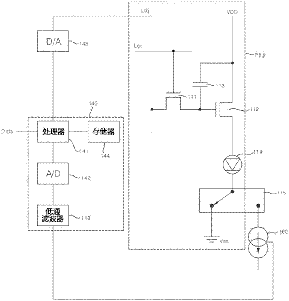
[0052] figure 2 is a circuit diagram schematically illustrating the configuration of a display according to Embodiment 1 of the present invention.

[0053] Such as figure 2 As shown, the display according to Embodiment 1 includes a display unit 100, a controller 120, a gate driver 130, a data driver 150, an anode driver 170, a selection switch 115, a current sink 160, an analog-to-digital converter 142 and a digital-to-analog converter 145.

[0054] The display unit 100 includes a plurality of gate lines Lg1 to Lgn (n is an integer greater than or equal to 2), a plurality of data lines Ld1 to Ldm (m is an integer greater than or equal to 2) arranged in parallel with each other, and a plurality of anode lines La1 to Lan. A plurality of gate lines Lg1 to Lgn and a plurality of anode lines La1 to Lan are respectively arranged in parallel to each other. In addition, the plurality of data lines Ld1 to Ldm cross the plurality of gate lines Lg1 to Lgn and the plurality of anode...

Embodiment 2

[0102] Next, Embodiment 2 of the present invention will be described. Figure 5 is a circuit diagram schematically illustrating the configuration of an organic light emitting display according to Embodiment 2 of the present invention.

[0103] Such as Figure 5 As shown, the organic light emitting display according to Embodiment 2 includes a display unit 200 , a selection switch 215 , a current sink 260 , a current measurement circuit 240 , a variation value compensation unit 220 and a data driver 250 . although Figure 5 Not shown in , the organic light emitting display includes known components, for example, a gate driver applying a selection signal on each gate line Lgi, supplying a driving voltage from a first voltage source VDD to an anode on each anode line Lai Drivers, controllers that control each unit of the display, etc.

[0104] The display unit 200 includes a plurality of gate lines Lg1 to Lgn (n is an integer greater than or equal to 2), a plurality of data lines...


PUM


Abstract

The present invention relates to a compensation apparatus, which compensates for a brightness deviation due to use of an organic light emitting display device for a long time, comprising: a driving transistor (112) having a first electrode, a second electrode and a gate electrode; a first voltage source (VDD) connected to the first electrode of the driving transistor (112); an organic electroluminescence device (114) having an anode electrode connected to the second electrode of the driving transistor (112); a second voltage source (Vss); a selection switch (115) for selectively connecting a cathode electrode of the organic electroluminescence device (114) between the second voltage source (Vss) and a current sink (160); and a current measurement circuit (140) for measuring the current flowing from the first voltage source (VDD) to the current sink (160) when a test voltage (Vdata) is applied to the gate electrode of the driving transistor (112).

Description

technical field [0001] The present invention relates to a brightness deviation compensation device and compensation method of a display, and more particularly, to a brightness deviation compensation device and a compensation method of an organic electroluminescence device of a display device using an organic electroluminescence device as a pixel of the display. Background technique [0002] Recently, an organic electroluminescent display (hereinafter also simply referred to as an "organic light emitting display") using an organic electroluminescent device (hereinafter referred to as an "organic EL device") as a pixel of the display has drawn attention. Herein, an organic light emitting display using an organic electroluminescent device as a light emitting device is light and thin, and has superior luminance characteristics and viewing angle characteristics than other displays, and thus is expected to be a next-generation flat panel display device. [0003] An organic electro...

Claims


Application Information

Patent Timeline
Patent Type & Authority Applications(China)
IPC IPC(8): G09G3/3258
CPCG09G3/3258G09G2300/0842G09G2300/0861G09G2300/0866G09G2320/0295G09G2320/045G09G2320/0693
Inventor 李正哲
Owner NEOVIEWKOLON
Why Eureka
Try Eureka