CMOS reference voltage source without Bipolar transistors

A reference voltage source and transistor technology, applied in the field of reference voltage source and CMOS reference voltage source, can solve the problems of poor performance, complex structure and high power consumption, and achieve the effect of extremely high power consumption, good performance and low power consumption

Active Publication Date: 2016-04-06
GUILIN UNIV OF ELECTRONIC TECH
View PDF7 Cites 11 Cited by
  • Summary
  • Abstract
  • Description
  • Claims
  • Application Information

AI Technical Summary

Problems solved by technology

[0004] In view of the incompatibility between the above-mentioned existing reference voltage source and the standard CMOS process, and the defects of large power consumption, complex structure, and poor performance, the technical problem to be solved by the present invention is to provide a nanowatt-level power supply with a high power supply rejection ratio CMOS reference voltage source without Bipolar transistor, it can work in the subthreshold region

Method used


Image

  • CMOS reference voltage source without Bipolar transistors
  • CMOS reference voltage source without Bipolar transistors
  • CMOS reference voltage source without Bipolar transistors

Examples


Embodiment Construction

[0028] The present invention will be further explained below in conjunction with the accompanying drawings and specific embodiments, but it is not intended to limit the present invention.

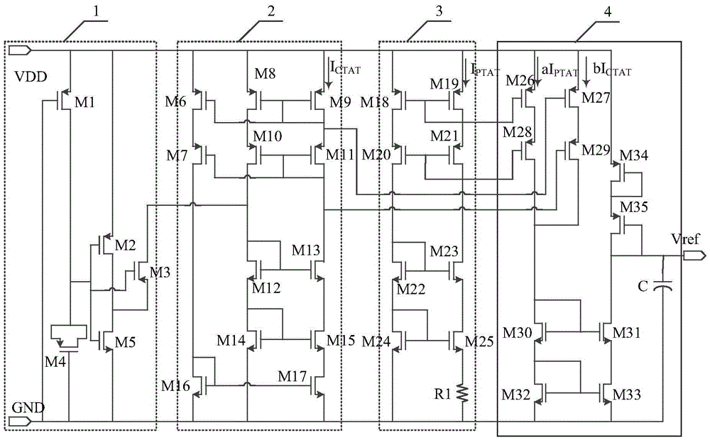
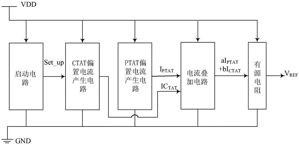
[0029] Such as figure 2 As shown, a CMOS reference voltage source without Bipolar transistors includes a start-up circuit 1 connected in parallel between the power supply VDD and the ground GND, a CTAT voltage generation circuit 2, a PTAT voltage generation circuit 3, and a current superposition circuit 4; wherein

[0030] The output terminal of the start-up circuit 1 is connected to the CTAT voltage generating circuit, which is used to provide the start-up current of the reference voltage source, so that the reference voltage source gets rid of the degeneracy bias point;

[0031] The output terminal of the CTAT voltage generation circuit 2 is connected with the current superposition circuit 4; the output terminal of the PTAT voltage generation circuit 3 is connected with the current super...


PUM


Abstract

The invention discloses a CMOS reference voltage source without Bipolar transistors. The CMOS reference voltage source comprises a starting circuit which is connected between a power source (VDD) and the ground (GND) in parallel, a CTAT voltage generating circuit, a PTAT voltage generating circuit and a current superposed circuit; the output end of the starting circuit is connected with the CTAT voltage generating circuit and used for making the reference voltage source break away from a degeneracy bias point when a power source powers up; the output end of the CTAT voltage generating circuit is connected with the current superposed circuit; the output end of the PTAT voltage generating circuit is connected with the current superposed circuit; the current superposed circuit is used for superposing a current generated in the CTAT voltage generating circuit and a current generated in the PTAT voltage generating circuit, so that a current source having the zero temperature drift is obtained, and the current source generates the reference voltage (Vref) through an active subcircuit. By the adoption of the CMOS reference voltage source with the mentioned composition, BJT and diodes are not used, influence of temperature variation can be eliminated, complete compatibility with a standard CMOS process is achieved, system cost is effectively lowered, and the CMOS reference voltage source has the advantages of being extremely low in power consumption, high in power supply rejection ratio and good in performance.

Description

technical field [0001] The invention relates to a reference voltage source, in particular to a CMOS reference voltage source without a Bipolar transistor, and belongs to the technical field of integrated circuit design. Background technique [0002] The reference voltage source is an important module in analog integrated circuits, digital-analog mixed-signal integrated circuits, and system integrated chips. The purpose of applying references is to establish a DC voltage that is independent of power supply and process and has definite temperature characteristics. [0003] With the rapid development of the wireless communication industry and the wide application of portable electronic products, low-power power supplies have become more and more important. As an important component of the power supply, the voltage reference source has great influence on power consumption and stability on the performance of the circuit. All have great influence. With the continuous improvement ...

Claims


Application Information

Patent Timeline
Patent Type & Authority Applications(China)
IPC IPC(8): G05F3/26
CPCG05F3/262
Inventor 岳宏卫邓进丽朱智勇段吉海韦雪明郑龙王宏庆
Owner GUILIN UNIV OF ELECTRONIC TECH
Why Eureka
Try Eureka