Color filter based on rectangular lattice arrangement and preparation method and application thereof
A technology of color filter and lattice arrangement, which is applied in the field of color filter, can solve the problem that the color response of high saturation cannot be stably realized, and achieve excellent incident angle insensitivity, high saturation, and promote development Effect
- Summary
- Abstract
- Description
- Claims
- Application Information
AI Technical Summary
Problems solved by technology
Method used
Image
Examples
Embodiment 1
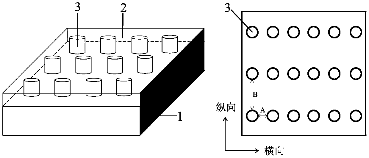
[0051] refer to figure 1 , an example of a color filter based on a rectangular lattice arrangement designed by the present invention, including: a transparent substrate 1, a transparent covering layer 2 and nano-pillars 3; wherein, the material of the transparent substrate 1 is glass; the The material of the transparent covering layer 2 is PMMA; the material of the nano-column array 3 is hydrogenated amorphous silicon.
[0052] The nano-column 3 is cylindrical, its height is between 50-120nm, and its diameter is between 80-140nm, it is fixed on the upper surface of the transparent substrate 1, and the transparent covering layer 2 is filled on the nano-column 3 , and the nano-columns 3 are coated in the transparent covering layer 2; the array formed by the nano-columns 3 is arranged in a rectangular lattice, that is, the lateral period is different from the vertical period, specifically shown as: the distance between adjacent nano-columns A (horizontal period) and the shortest...
Embodiment 2
[0054] 1. Preparation of color filters based on rectangular lattice arrangement, the steps are:
[0055] First, with the help of silane (SiH 4 ) and helium (He) to achieve the deposition of hydrogenated amorphous silicon with a height of 80 nm on a transparent substrate by plasma enhanced chemical vapor deposition (PECVD).
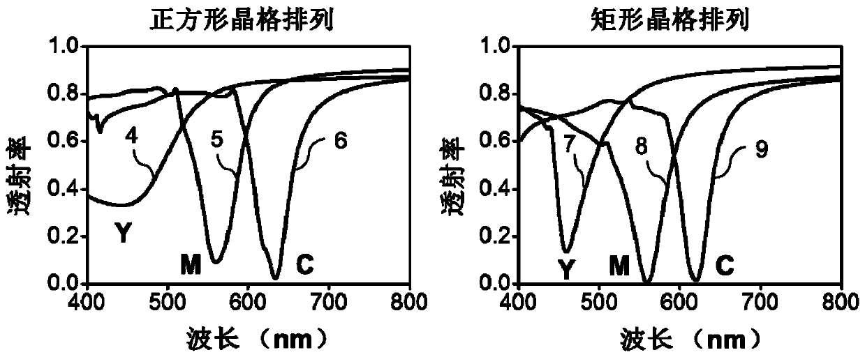
[0056] Subsequently, photoresist nanocolumn arrays with different nanocolumn sizes and periods were formed on the hydrogenated amorphous silicon film by means of electron beam lithography. The diameter / lateral period / vertical period of the photoresist nanocolumn array are 180nm / 370nm / 400nm, 140nm / 260nm / 350nm and 80nm / 150nm / 300nm, respectively, corresponding to the nanocolumn period and diameter of the CMY filter.
[0057] Then, with CHF 3 and SF 6 The mixed gas is dry-etched in the plasma etching machine to etch away the excess hydrogenated amorphous silicon exposed, and the residual photoresist is removed by the oxidizing plasma in the etching machine ...
Embodiment 3
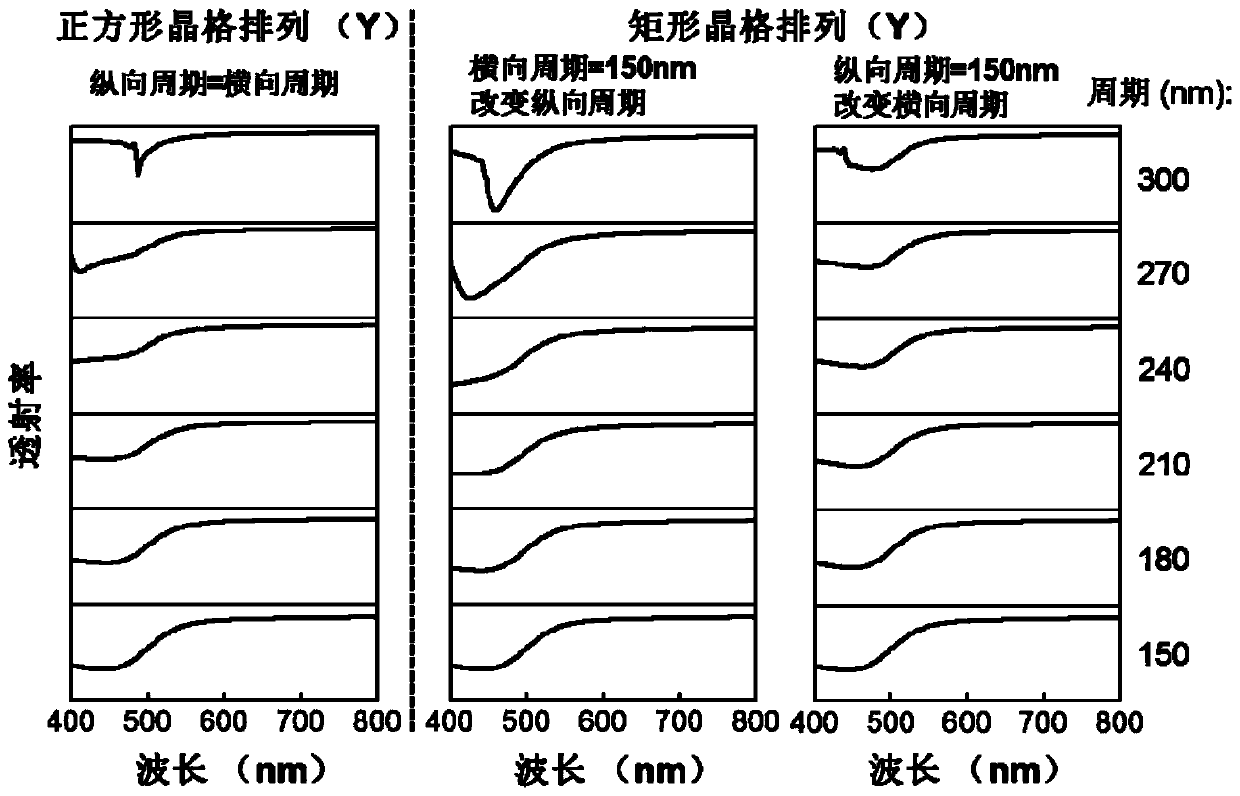
[0065] The method for preparing the color filter in this embodiment is the same as in Example 2, the difference is that the period of the yellow filter of the square and rectangular lattice arrays is increased from 150nm to 300nm; wherein, for the square lattice arrangement, the vertical period and the transverse The periods are increased at the same time and by the same increment. For the arrangement of rectangular lattices, the horizontal (or vertical) period is fixed and only the vertical (or horizontal) period is changed.
[0066] Performance Testing:
[0067] image 3 The transmission spectrum of the yellow filter (Y) based on the square lattice arrangement and the rectangular lattice arrangement prepared in this embodiment varies with the period, from image 3 The change trend of the transmission spectrum shown in the left figure shows that although the resonance wavelength of the yellow filter based on the square lattice arrangement does not change greatly with the ...
PUM
| Property | Measurement | Unit |
|---|---|---|
| height | aaaaa | aaaaa |
| diameter | aaaaa | aaaaa |
| diameter | aaaaa | aaaaa |
Abstract
Description
Claims
Application Information


