Supercharge Your Innovation With Domain-Expert AI Agents!

Light emitting diode and manufacturing method therefor

A manufacturing method and gallium polarity technology, applied in electrical components, circuits, semiconductor devices, etc., can solve problems such as poor stability of chip voltage reliability, and achieve the effect of solving the problem of ohmic contact stability and ensuring voltage reliability.

Active Publication Date: 2016-04-13
XIAMEN SANAN OPTOELECTRONICS TECH CO LTD
View PDF5 Cites 8 Cited by
  • Summary
  • Abstract
  • Description
  • Claims
  • Application Information

AI Technical Summary

Problems solved by technology

[0004] In view of the above problems, the present invention provides a vertical light-emitting diode with good n-type ohmic contact and its manufacturing method to overcome the problem of chip voltage reliability caused by the poor stability of the n-face GaN ohmic contact electrode existing in the existing vertical chip

Method used


Image

  • Light emitting diode and manufacturing method therefor
  • Light emitting diode and manufacturing method therefor
  • Light emitting diode and manufacturing method therefor

Examples


Embodiment Construction

[0022] The present invention will be further described below in conjunction with the accompanying drawings and preferred specific embodiments. In specific device design and manufacture, the LED structure proposed by the present invention can be modified within a certain range in part of the structure and size according to the needs of the application field and process implementation, and the selection of materials can be flexible.

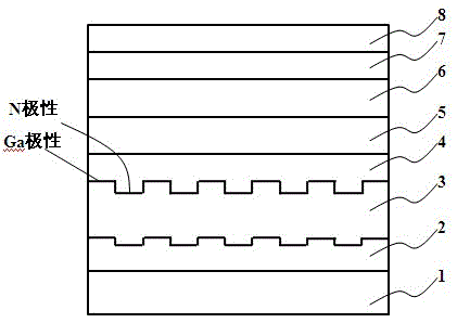
[0023] figure 1 It is a schematic cross-sectional view of an LED epitaxial structure for a vertical structure implemented according to the present invention.

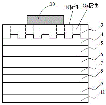
[0024] see figure 1 , an LED epitaxial structure, including from bottom to top: substrate 1, u-type nitride layer 2, n-type nitride layer 3, n-type recovery layer 4, n-type superlattice structure layer 5, active layer 6. A p-type nitride layer 7 and a p-type contact layer 8 .

[0025] Among them, the preferred sapphire for the substrate 1 has a planar surface structure. The upper surface...


PUM


Abstract

The invention discloses an LED epitaxial structure, a chip structure and a manufacturing method therefor. The chip comprises a conductive substrate, a p type nitride layer, an active layer, an n type recovery layer, an n type nitride layer and an n electrode from the bottom up in sequence, wherein the n type nitride layer is provided with a nitrogen polarity crystal and a gallium polarity crystal; a height difference exists between the surfaces of the nitrogen polarity region and the gallium polarity region; mixed polarity that is consistent with that of the n type nitride layer exists on the surface of one side, adjacent to the n type nitride layer, of the n type recovery layer; and the connected gallium polarity surface is arranged on the surface of one side, far from the contacted n type nitride layer, of the n type recovery layer.

Description

technical field [0001] The invention relates to the field of semiconductors, in particular to a vertical light-emitting diode with good n-type ohmic contact and a manufacturing method thereof. Background technique [0002] In recent years, with the maturity of substrate transfer technology, vertical structure chip technology has been more and more used in the industry. It generally deposits GaN-based thin films on sapphire substrates by MOCVD, and then deposits GaN-based thin films through wafer bonding technology. Or electroplating technology to bond to the semiconductor or metal substrate, and then peel off the sapphire substrate. This technology effectively improves the luminous efficiency of GaN-based LED chips due to its high light extraction efficiency, current expansion capability and thermal conductivity, especially in the field of high current density and high power applications. [0003] However, in the above-mentioned vertical structure chip technology, the surfa...

Claims


Application Information

Patent Timeline
Patent Type & Authority Applications(China)
IPC IPC(8): H01L33/32H01L33/00
CPCH01L33/16H01L33/0075H01L33/12H01L33/32H01L33/325
Inventor 张洁朱学亮杜成孝刘建明徐宸科
Owner XIAMEN SANAN OPTOELECTRONICS TECH CO LTD
Features
  • R&D
  • Intellectual Property
  • Life Sciences
  • Materials
  • Tech Scout
  • Unparalleled Data Quality
  • Higher Quality Content
  • 60% Fewer Hallucinations
Learn More