Group-III nitride semiconductor epitaxial substrate, group-III nitride semiconductor light-emission element, and production method for these

A technology of nitride semiconductors and epitaxial substrates, which is applied in semiconductor/solid-state device manufacturing, semiconductor devices, semiconductor lasers, etc., can solve problems such as lattice constants, different thermal expansion coefficients, large strains, and difficulty in obtaining atomic-level surface flatness. Achieves the effect of suppressing crack generation and excellent surface flatness

Active Publication Date: 2016-04-13
DOWA ELECTRONICS MATERIALS CO LTD
View PDF5 Cites 8 Cited by
  • Summary
  • Abstract
  • Description
  • Claims
  • Application Information

AI Technical Summary

Problems solved by technology

However, the lattice constant and thermal expansion coefficient of Group III nitride semiconductors and these substrates are quite different.
Therefore, when a Group III nitride semiconductor is grown on these substrates, due to various reasons such as lattice mismatch and a difference in thermal expansion coefficient, the strain of the Group III nitride semiconductor formed on the substrate becomes large, and it is difficult to obtain atomic Excellent surface flatness

Method used


Image

  • Group-III nitride semiconductor epitaxial substrate, group-III nitride semiconductor light-emission element, and production method for these
  • Group-III nitride semiconductor epitaxial substrate, group-III nitride semiconductor light-emission element, and production method for these
  • Group-III nitride semiconductor epitaxial substrate, group-III nitride semiconductor light-emission element, and production method for these

Examples


Embodiment

[0095] (trial example 1)

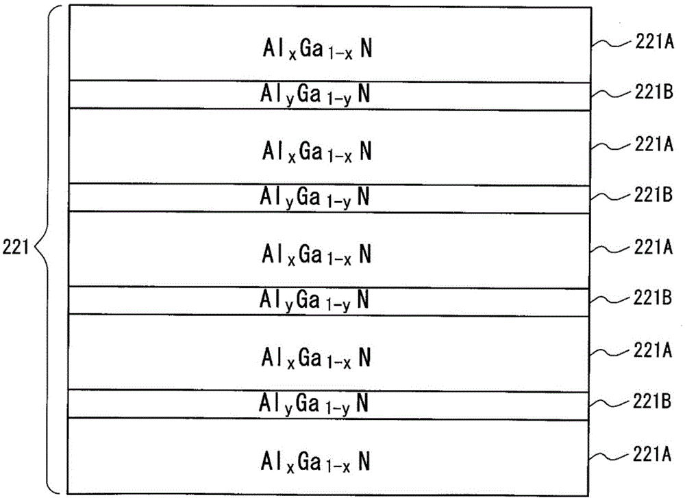
[0096] AlN prepared to form an undoped AlN layer (thickness: 600nm, half-value width of the AlN (102) plane according to XRC (X-ray rocking curve; X-ray Rocking Curve): 242 seconds) on a sapphire substrate (thickness: 430 μm) template substrate. Using the MOCVD method on this AlN template substrate, flow TMA: 11.5 sccm, NH at a pressure of 10kPa and a temperature of 1150°C 3 : 575sccm After forming a non-doped AlN layer with a thickness of 21.6nm, flow TMA: 11.5sccm, NH 3 : 575 sccm, SiH 4 : 50sccm, forming an impurity concentration of 2.0×10 19 / cm 3 Si-doped AlN buffer layer with a thickness of 5.4 nm. That is, an undoped AlN layer and a Si-doped AlN buffer layer are formed on an AlN template substrate. That is, when the sum of the layer thicknesses of the undoped AlN layer and the Si-doped AlN buffer layer on the AlN template substrate is 27 nm, the Si-doped thickness is 5.4 nm. Next, the first stacked body, the second stacked body, and the...


PUM

PropertyMeasurementUnit
thicknessaaaaaaaaaa
thicknessaaaaaaaaaa
thicknessaaaaaaaaaa

Abstract

Provided are: a group-III nitride semiconductor epitaxial substrate which exhibits superior surface smoothness while inhibiting crack formation and a problem in which the shape of the EL spectrum thereof forms double peaks; a group-III nitride semiconductor using said substrate; and a production method for these. A group-III nitride semiconductor epitaxial substrate (100) according to the present invention is characterized by being provided with: a substrate (112) in which at least a surface section thereof comprises AlN; an undoped AlN layer (114) formed upon the substrate (112); an Si-doped AlN buffer layer (116) formed upon the undoped AlN layer (114); and a superlattice stacked body (120) formed upon the Si-doped AlN buffer layer (116). The group-III nitride semiconductor epitaxial substrate (100) is further characterized in that the Si-doped AlN buffer layer (116) has an Si concentration of at least 2.0*1019/cm3, and a thickness of 4-10 nm.

Description

technical field [0001] The present invention relates to a Group III nitride semiconductor epitaxial substrate, a Group III nitride semiconductor light-emitting element, and their manufacturing methods. Background technique [0002] In recent years, in general, Group III nitride semiconductors composed of compounds of Al, Ga, In, etc. and N have been widely used in light-emitting elements, elements for electronic devices, and the like. The characteristics of such a device are largely influenced by the atomic-level surface flatness of the Group III nitride semiconductor, and therefore a technique for growing a Group III nitride semiconductor having excellent surface flatness is required. [0003] Group III nitride semiconductors are formed by epitaxial growth on a substrate made of sapphire, SiC, Si, GaAs, or the like. However, the Group III nitride semiconductor and these substrates differ greatly in lattice constant and thermal expansion coefficient. Therefore, when a Grou...

Claims


Application Information

Patent Timeline
Patent Type & Authority Applications(China)
IPC IPC(8): H01L21/205H01L33/12H01L33/32H01S5/343
CPCH01L33/12H01L33/32H01L33/007H01L21/02458H01L21/02507H01L21/0254H01L21/02576H01L21/0262C30B29/403C30B29/68H01S5/34333H01S2301/173H01L33/04H01L33/06H01L33/325
Inventor 岩田雅年大鹿嘉和
Owner DOWA ELECTRONICS MATERIALS CO LTD
Why Eureka
Try Eureka