Method for manufacturing SOI substrate

a technology of soi and substrate, which is applied in the direction of basic electric elements, electrical apparatus, semiconductor devices, etc., can solve the problems of remarkable processing time, temperature increase in accordance with ion irradiation, and difficult shortening processing time, so as to improve the planarity of the surface of a single crystal semiconductor layer after separation, and improve throughput. , the effect of improving the separation speed

Inactive Publication Date: 2012-03-27
SEMICON ENERGY LAB CO LTD
View PDF13 Cites 8 Cited by
  • Summary
  • Abstract
  • Description
  • Claims
  • Application Information

AI Technical Summary

Benefits of technology

[0009]On the other hand, in the case where a non-mass-separation type ion irradiation method is used, although throughput is significantly improved as compared to the case where a mass-separation type ion irradiation method is used, a problem arises in that temperature increase is larger in accordance with ion irradiation as compared to the case where an ion implantation method is used because a large area of a substrate can be irradiated at a time. Such temperature increase of the substrate promotes thermal diffusion of an element derived from added ions in the substrate and becomes a factor which broadens distribution of the ions in a depth direction. In addition, the temperature increase of the substrate promotes desorption of the element derived from the ions added to and existing in the substrate.
[0020]According to an embodiment of the disclosed invention, in a method for manufacturing an SOI substrate, throughput can be improved and planarity of a surface of a single crystal semiconductor layer after separation can be improved.

Problems solved by technology

However, in the above hydrogen ion implantation separation method, since a mass-separation type ion irradiation method (an ion implantation method) by which a silicon wafer is irradiated with ions which are generated from a source gas and are subjected to mass separation, a range of an area in which the silicon wafer is irradiated with the ions is small and it is difficult to shorten processing time.
In particular, as the silicon wafer is increased, a problem of processing time becomes remarkable.
On the other hand, in the case where a non-mass-separation type ion irradiation method is used, although throughput is significantly improved as compared to the case where a mass-separation type ion irradiation method is used, a problem arises in that temperature increase is larger in accordance with ion irradiation as compared to the case where an ion implantation method is used because a large area of a substrate can be irradiated at a time.
Therefore, a problem arises in that a single crystal semiconductor substrate is not uniformly irradiated with the ions.
As described above, if the distribution of the element derived from the added ions is broadened, it is difficult to separate the semiconductor substrate favorably.

Method used


Image

  • Method for manufacturing SOI substrate
  • Method for manufacturing SOI substrate
  • Method for manufacturing SOI substrate

Examples


embodiment 1

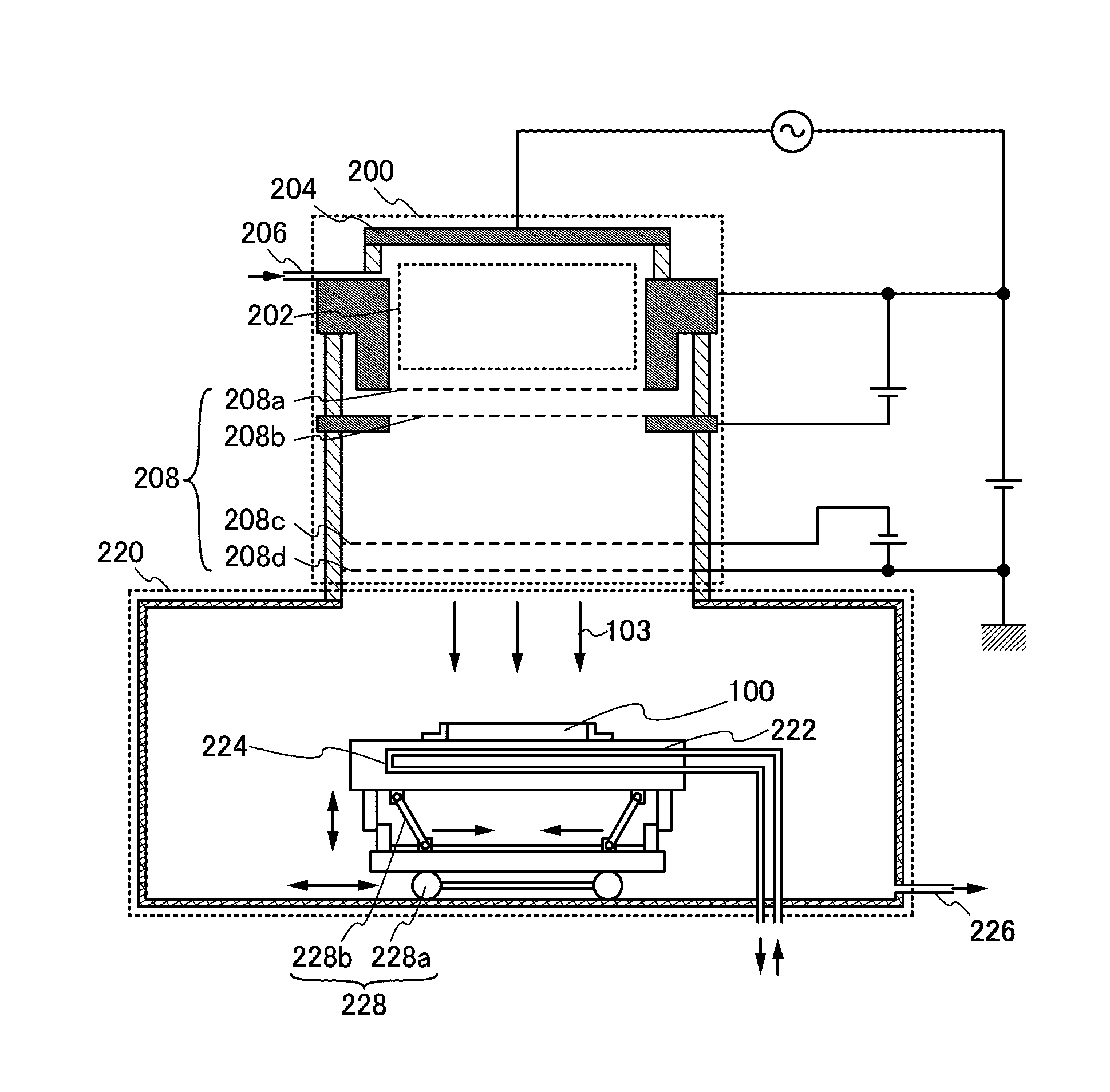
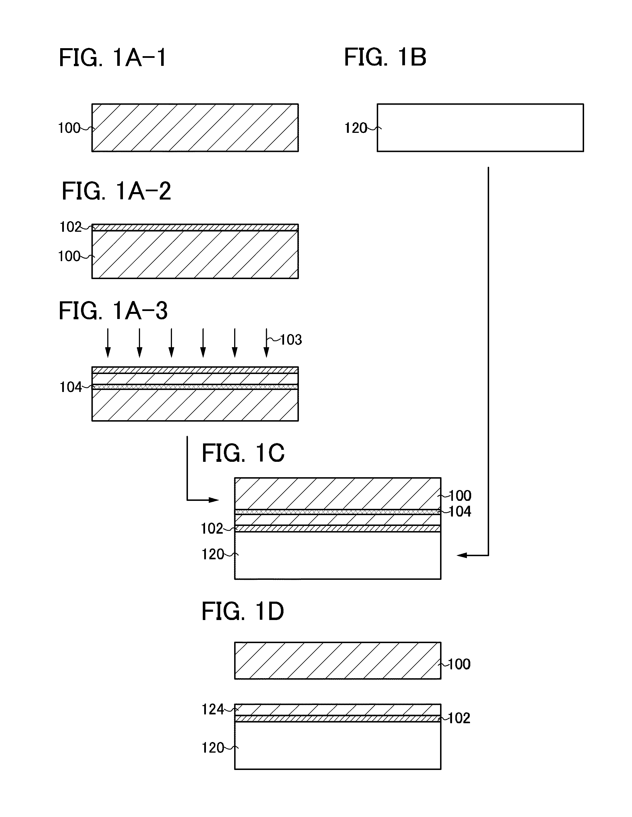
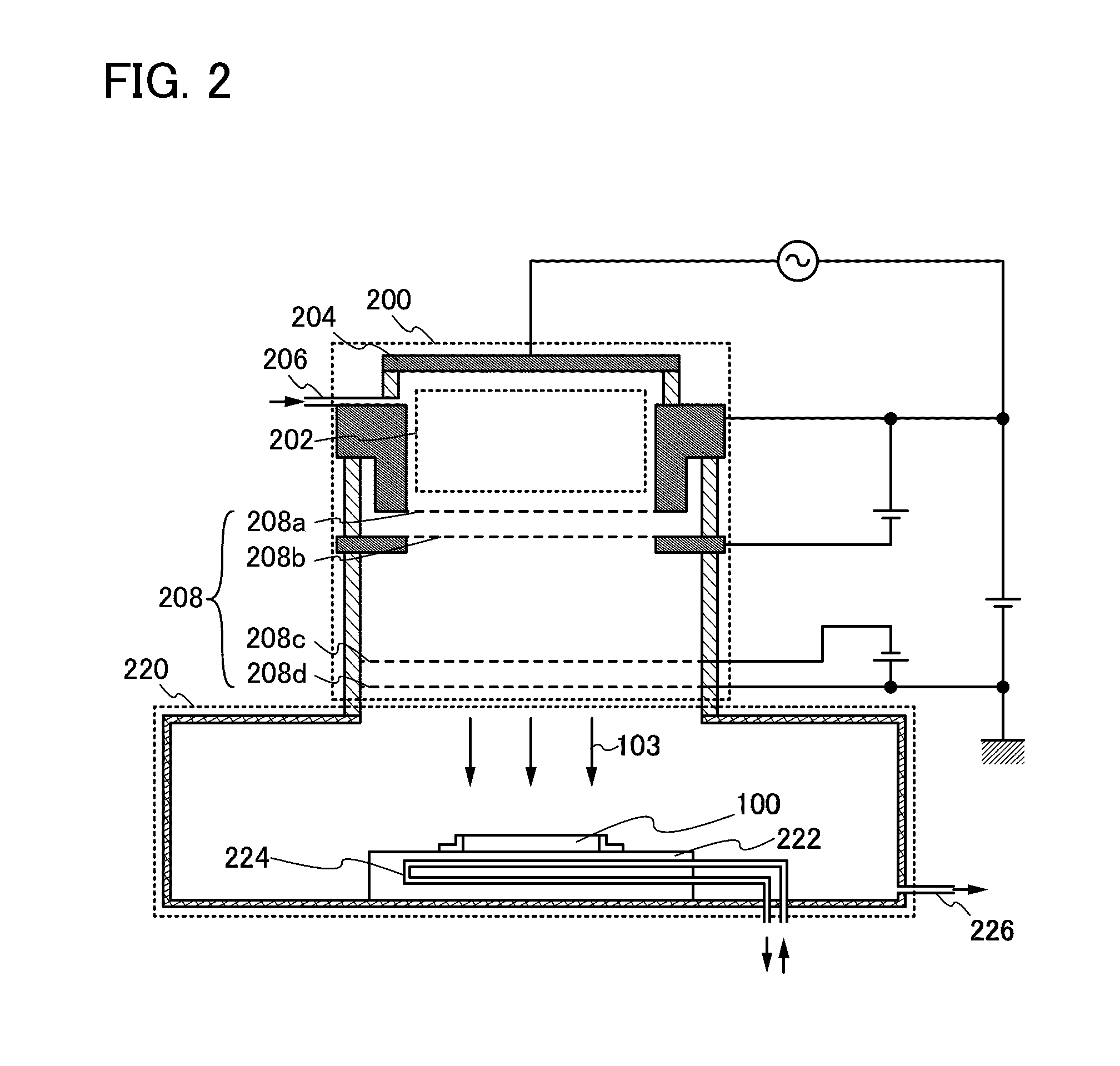
[0034]In this embodiment, an example of a method for manufacturing an SOI substrate will be described with reference to drawings.

[0035]First, a single crystal semiconductor substrate 100 is prepared (see FIG. 1A-1).

[0036]As the single crystal semiconductor substrate 100, a single crystal semiconductor substrate formed using an element belonging to Group 14, such as a single crystal silicon substrate, a single crystal germanium substrate, or a single crystal silicon germanium substrate, can be used. Alternatively, a compound semiconductor substrate formed of gallium arsenide, indium phosphide, or the like may be used. The size of a commercial silicon substrate is typically 5 inches (125 mm) in diameter, 6 inches (150 mm) in diameter, 8 inches (200 mm) in diameter, 12 inches (300 mm) in diameter, and 16 inches (400 mm) in diameter, and a typical shape thereof is a circular shape. Note that the shape of the single crystal semiconductor substrate 100 is not limited to a circular shape, ...

embodiment 2

[0079]In this embodiment, a method for cooling the single crystal semiconductor substrate 100 in performing ion irradiation, which is different from that in the above embodiment, is described.

[0080]As described above, in the case where an ion doping method is used, a large area is irradiated with ions at a time; therefore, the temperature of the single crystal semiconductor substrate 100 is increased. Accordingly, as the ion irradiation time increases, the temperature of the single crystal semiconductor substrate 100 increases. That is, there is a large difference between the temperature of the single crystal semiconductor substrate 100 at the time when ion irradiation is started and the temperature of the single crystal semiconductor substrate 100 at the time when ion irradiation is completed.

[0081]Therefore, at the time when ion irradiation is started, thermal diffusion of the element derived from the added ions hardly occurs; however, as irradiation with the ions proceeds, the te...

embodiment 3

[0089]In this embodiment, in the manufacturing method described in any of the above embodiments, a method for bonding the single crystal semiconductor substrate 100 and the base substrate 120 is described in detail with reference to the drawings.

[0090]First, the single crystal semiconductor substrate 100 is prepared (see FIG. 3A-1). Note that it is preferable that the surface of the single crystal semiconductor substrate 100 be cleaned as appropriate in advance using a sulfuric acid / hydrogen peroxide mixture (SPM), an ammonium hydroxide / hydrogen peroxide mixture (APM), a hydrochloric acid / hydrogen peroxide mixture (HPM), diluted hydrogen fluoride (DHF), or the like in terms of removing contamination. Further, diluted hydrogen fluoride and ozone water may be discharged alternately to clean the single crystal semiconductor substrate 100.

[0091]Next, an oxide film 132 is formed on the surface of the single crystal semiconductor substrate 100 (see FIG. 3A-2).

[0092]As the oxide film 132, ...


PUM


Abstract

The present invention provides a method for manufacturing an SOI substrate, to improve planarity of a surface of a single crystal semiconductor layer after separation by favorably separating a single crystal semiconductor substrate even in the case where a non-mass-separation type ion irradiation method is used, and to improve planarity of a surface of a single crystal semiconductor layer after separation as well as to improve throughput. The method includes the steps of irradiating a single crystal semiconductor substrate with accelerated ions by an ion doping method while the single crystal semiconductor substrate is cooled to form an embrittled region in the single crystal semiconductor substrate; bonding the single crystal semiconductor substrate and a base substrate with an insulating layer interposed therebetween; and separating the single crystal semiconductor substrate along the embrittled region to form a single crystal semiconductor layer over the base substrate with the insulating layer interposed therebetween.

Description

BACKGROUND OF THE INVENTION[0001]1. Field of the Invention[0002]The present invention relates to a method for manufacturing a substrate over which a semiconductor layer is provided with an insulating film interposed therebetween. In particular, the present invention relates to a method for manufacturing an SOI (silicon on insulator) substrate. In addition, the present invention relates to a method for manufacturing a semiconductor device using a substrate over which a semiconductor layer is provided with an insulating film interposed therebetween.[0003]2. Description of the Related Art[0004]In recent years, an integrated circuit using an SOI (silicon on insulator) substrate in which a thin single crystal semiconductor layer is formed on an insulating surface, instead of a bulk silicon wafer has been developed. Since parasitic capacitance between a drain of a transistor and a substrate is reduced by using the SOI substrate, the SOI substrate has attracted attention as one improving p...

Claims


Application Information

Patent Timeline
Patent Type & Authority Patents(United States)
IPC IPC(8): H01L21/331H01L21/8222
CPCH01L21/76254H01L27/1266H01L27/1214H01L29/66772H01L27/12H01L21/20
Inventor SHICHI, TAKESHIKOEZUKA, JUNICHIOHNUMA, HIDETOYAMAZAKI, SHUNPEI
Owner SEMICON ENERGY LAB CO LTD
Why Eureka
Try Eureka