Method for manufacturing sic single-crystal substrate for epitaxial sic wafer, and sic single-crystal substrate for epitaxial sic wafer

A technology of silicon carbide single crystal and epitaxial silicon carbide, which is applied in the direction of chemical instruments and methods, manufacturing tools, single crystal growth, etc., can solve problems such as difficult to deal with large devices, low epitaxial defect density, etc., and achieve characteristics and yield improvement, Excellent reproducibility and excellent surface flatness effect

Inactive Publication Date: 2015-10-14
SHOWA DENKO KK
View PDF7 Cites 10 Cited by
  • Summary
  • Abstract
  • Description
  • Claims
  • Application Information

AI Technical Summary

Problems solved by technology

Currently, these epitaxial defect densities per 1cm 2 The level is about several to about 10, but the number of epitaxial defects contained in the device needs to be substantially zero, so at present, it is difficult to manufacture devices with an area larger than about 5 mm square with a high yield
In order to reduce the above-mentioned epitaxial defects, the growth temperature during epitaxial growth, the ratio of the number of carbon atoms to the number of silicon atoms in the material gas flowing during the growth (C / Si ratio), and various conditions before growth are optimized. chemical research, but it is difficult to obtain 1~2 cells / cm stably 2 The following low epitaxial defect density conditions
[0006] Therefore, although epitaxial SiC wafers, which are expected to be used in devices in the future, can produce small-area devices with the current epitaxial defect density, it is difficult to deal with large-scale devices with an area of ​​about 5 mm square or more

Method used


Image

  • Method for manufacturing sic single-crystal substrate for epitaxial sic wafer, and sic single-crystal substrate for epitaxial sic wafer
  • Method for manufacturing sic single-crystal substrate for epitaxial sic wafer, and sic single-crystal substrate for epitaxial sic wafer
  • Method for manufacturing sic single-crystal substrate for epitaxial sic wafer, and sic single-crystal substrate for epitaxial sic wafer

Examples


Embodiment 1

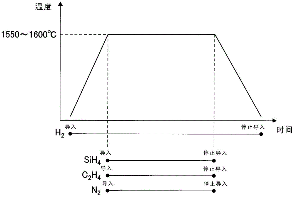
[0043] A 4-inch (100 mm) wafer is cut from a SiC single-crystal ingot with a thickness of about 400 μm, and subjected to grinding and normal polishing with diamond abrasive grains to prepare a substrate to be subjected to CMP. The polytype of this substrate is 4H type with an off angle of 4°. When polishing is performed in this way, the thickness of the processing-altered layer on the surface is about 100 nm or less. Next, perform CMP as follows.

[0044] As the polishing slurry, a slurry containing abrasive particles such as silicon dioxide and an acid is used, the processing pressure and the pH of the slurry are appropriately adjusted, and the polishing rate is 100 nm / hour, and the surface of the substrate is removed to a thickness of 100 nm ( The amount of polishing is 100 nm), and CMP is performed so that no polishing marks remain. After the completion of CMP, the pits on the surface of the SiC substrate obtained in this example were observed using a confocal microscope ...

Embodiment 2

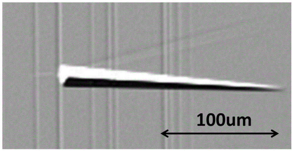
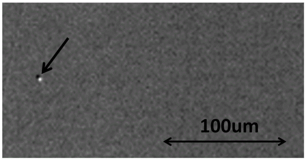
[0048] A SiC substrate of Example 2 was obtained in the same manner as in Example 1, except that the CMP polishing rate was 80 nm / hour and the polishing amount was 100 nm. On the surface of the SiC substrate after CMP, the density of approximately circular pits with a diameter of 0.5 μm to 1.5 μm and a depth of 50 nm to 500 nm is 0.6 pits / cm 2 . Next, epitaxial growth was carried out in the same manner as in Example 1, and the number of defects in the grown epitaxial film was evaluated. As a result, the carrot-shaped defect density was 0.8 defects / cm 2 , the density of all epitaxial defects including triangle defects and comet defects is 1.7 / cm 2 .

Embodiment 3

[0050] A SiC substrate of Example 3 was obtained in the same manner as in Example 1, except that the CMP polishing rate was 50 nm / hour and the polishing amount was 100 nm. On the surface of the SiC substrate after CMP, the density of approximately circular pits with a diameter of 0.5 μm to 1.5 μm and a depth of 50 nm to 500 nm is 0.4 pits / cm 2 . Next, epitaxial growth was carried out in the same manner as in Example 1, and the number of defects in the grown epitaxial film was evaluated. As a result, the carrot-shaped defect density was 0.6 defects / cm 2 , the density of all epitaxial defects including triangle defects and comet defects is 1.4 / cm 2 .


PUM

PropertyMeasurementUnit
thicknessaaaaaaaaaa
diameteraaaaaaaaaa
diameteraaaaaaaaaa

Abstract

 Provided is a method for manufacturing an SiC single-crystal substrate making it possible to obtain an epitaxial SiC wafer provided with a high-quality SiC single-crystal thin film devoid of surface defects, etc. Also provided is said SiC single-crystal substrate. A method for manufacturing an SiC single-crystal substrate for an epitaxial SiC wafer having a high-quality SiC single-crystal thin film devoid of surface defects, etc., wherein the surface of the SiC single-crystal substrate is polished using chemical-mechanical polishing (CMP) at a speed of no more than 100 nm / hr to remove the surface in a thickness of 100 nm or greater, and produce no more than 1 substantially round pit per cm2, the pit having a diameter of 0.5-1.5 µm and a depth of 50-500 nm

Description

technical field [0001] The invention relates to a method for manufacturing a silicon carbide single crystal substrate for an epitaxial silicon carbide wafer and a silicon carbide single crystal substrate for an epitaxial silicon carbide wafer. Background technique [0002] Silicon carbide (hereinafter referred to as SiC) is excellent in heat resistance and mechanical strength, and is physically and chemically stable, and thus attracts attention as an environment-resistant semiconductor material. In addition, in recent years, there has been an increasing demand for epitaxial SiC wafers as substrates for high-frequency, high-voltage electronic devices and the like. [0003] In the case of using epitaxial SiC wafers to produce power devices, high-frequency devices, etc., the following method is used: Usually, SiC thin films are deposited on SiC single crystal substrates (hereinafter referred to as SiC substrates) by thermal CVD (thermochemical vapor deposition) Epitaxial growt...

Claims


Application Information

Patent Timeline
Patent Type & Authority Applications(China)
IPC IPC(8): H01L21/205C30B25/20C30B29/36H01L21/304
CPCC30B25/20B24B37/042C30B25/186C30B29/36H01L21/02019H01L21/02024H01L21/02378H01L21/02529H01L21/0262H01L21/02658H01L29/1608Y10T428/24355B24B1/00H01L21/304
Inventor 蓝乡崇伊藤涉藤本辰雄
Owner SHOWA DENKO KK
Why Eureka
Try Eureka