Liquid crystal base image and wavefront dual-mode electrical-modulation imaging detection chip

An image-based, liquid crystal technology, applied in the field of imaging detection, can solve difficult remote sensing imaging satellite imaging observation and monitoring, flexible response and modulation, inability to use real-time image information for corrective capture and processing, optical device volume, quality and power consumption It can achieve the effect of good adaptability to the target and the environment, high accuracy of mapping and wavefront measurement, and high wavefront measurement accuracy.

Active Publication Date: 2016-04-20
HUAZHONG UNIV OF SCI & TECH
View PDF9 Cites 3 Cited by
  • Summary
  • Abstract
  • Description
  • Claims
  • Application Information

AI Technical Summary

Problems solved by technology

[0003] Generally speaking, it is difficult to make a qualitative breakthrough in the short term in terms of imaging and detection capabilities for complex targets and environments in the method of separately performing mapping and wavefront measurement and adjustment. The main defects are as follows: (1) Widely used in the observation of natural Adaptive imaging system based on wavefront measurement and adjustment of astronomical and astronomical phenomena, the volume, mass and power consumption of the optical device are relatively large, the imaging efficiency is relatively low, the equipment is expensive, and the cost of imaging is high; (2) through small / micro The imaging equipment should deal with the effects of image degradation, distortion, distortion, distortion or disappearance guided, induced or stimulated by artificial activities. Since the wavefront and its evolution data are obtained based on the wavefront measurement equipment configured separately, it cannot be used for real-time image information. (3) Under the condition of strict constraints on the size and power consumption of the device, it is difficult to accurately obtain the associated wavefront of the image in real time for image processing because the imaging and wavefront measurement and adjustment are performed separately. Functional processing, such as image / terminal / guided hypersonic vehicles, fast maneuvering targets or hypersonic moving targets, etc., which are typical and difficult to sensitively respond to and adjust the track or attack path based on the existing wavefront measurement and adjustment methods. (4) It is difficult to flexibly respond and adjust the imaging observation and monitoring of remote sensing imaging satellites working in low and medium orbits based on wavefront measurement and adjustment; (5) Imaging of femtosecond chemical and physical processes of biochemical molecules (6) The imaging optical system that performs mapping and wavefront measurement and adjustment with a common optical aperture needs to be loaded with a wavefront measurement and adjustment system, which brings equipment volume, cost and performance, etc. Many intrinsic problems; (7) Imaging systems based on wavefront measurement and adjustment are still difficult to miniaturize / miniaturize

Method used


Image

  • Liquid crystal base image and wavefront dual-mode electrical-modulation imaging detection chip
  • Liquid crystal base image and wavefront dual-mode electrical-modulation imaging detection chip
  • Liquid crystal base image and wavefront dual-mode electrical-modulation imaging detection chip

Examples


Embodiment Construction

[0024] In order to make the object, technical solution and advantages of the present invention clearer, the present invention will be further described in detail below in conjunction with the accompanying drawings and embodiments. It should be understood that the specific embodiments described here are only used to explain the present invention, not to limit the present invention. In addition, the technical features involved in the various embodiments of the present invention described below can be combined with each other as long as they do not constitute a conflict with each other.

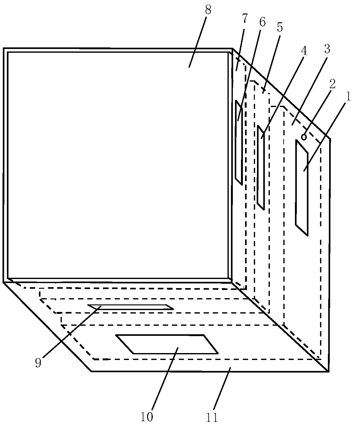
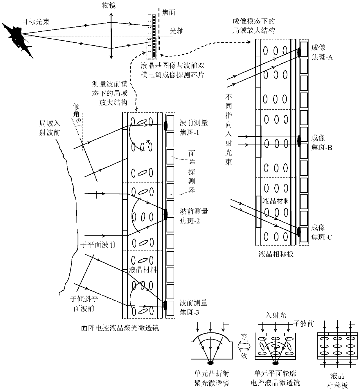
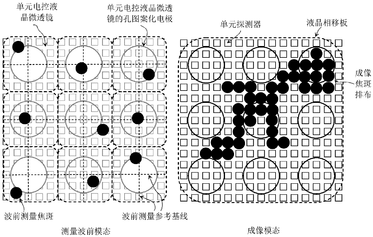
[0025] figure 1 It is a schematic structural diagram of a liquid crystal-based image and wavefront dual-mode electrical modulation imaging detection chip according to an embodiment of the present invention. The liquid crystal-based image and wavefront dual-mode electrical modulation imaging detection chip of the embodiment of the present invention includes: an image and wavefront dual-mode elec...


PUM


Abstract

The invention discloses a liquid crystal base image and wavefront dual-mode electrical-modulation imaging detection chip, and the chip comprises a liquid crystal micro-optical structure, an area-array visible-light detector and a drive control preprocessing module; the liquid crystal micro-optical structure is an area-array electronic control liquid crystal micro lens under a sequential power-up state; the area-array visible-light detector is divided into a plurality of sub-area array visible-light detectors by the area-array electronic control liquid crystal micro lens according to the array size thereof, and each unit of the electronic control liquid crystal micro lens matches one sub-area array visible-light detector to form a wavefront measurement mode; the liquid crystal micro-optical structure is a liquid crystal phase plate for delaying an incident wave beam under a sequential power-off state, and the liquid crystal phase plate and the area-array visible-light detector form an imaging mode. According to the invention, the chip can capture the emerging wavefront and a high image quality flat image of a target based on a sequential electric signal, the detection efficiency is high, the chip is easy to use and couple with a conventional imaging optical system.

Description

technical field [0001] The invention belongs to the technical field of imaging detection, and more specifically relates to a detection chip for controlling a liquid crystal micro-optical structure based on time-sequential electrical signals to realize wavefront measurement and high-quality imaging. Background technique [0002] The wavefront is a basic parameter used to characterize the light wave in the transport state, which is closely related to the spatial propagation behavior of the light wave, the energy transport efficiency, and the energy spatial correlation distribution form of the fluctuating light field. For the imaging system based on the acquisition of the spatial difference distribution of energy transport in the target light field, the quality of the image is subject to many factors, including the properties of the target light field, the beam transmission behavior in the environmental medium, and the energy difference of the optical system. Gathering ability,...

Claims


Application Information

Patent Timeline
Patent Type & Authority Applications(China)
IPC IPC(8): G01J5/00
CPCG01J5/00G01J2005/0077
Inventor 张新宇雷宇信钊炜魏冬桑红石王海卫谢长生
Owner HUAZHONG UNIV OF SCI & TECH
Why Eureka
Try Eureka