
Exposure development method for circuit board

A technology of exposure and development, circuit board, applied in the directions of printed circuit, printed circuit manufacturing, electrical components, etc., can solve the problems of poor pattern uniformity and poor pattern accuracy, and achieve the effect of avoiding exposure and improving pattern accuracy and pattern uniformity.

Active Publication Date: 2016-04-27
SHENNAN CIRCUITS
View PDF3 Cites 2 Cited by
  • Summary
  • Abstract
  • Description
  • Claims
  • Application Information

AI Technical Summary

Problems solved by technology

[0005] The embodiment of the present invention provides a method for exposure and development of circuit boards to solve the problems in the prior art when exposing groove bottom patterns, such as poor exposure, poor pattern accuracy, and poor pattern uniformity.

Method used


Image

  • Exposure development method for circuit board
  • Exposure development method for circuit board
  • Exposure development method for circuit board

Examples


Embodiment 1

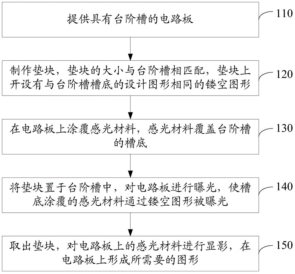
[0023] Please refer to figure 1 , an embodiment of the present invention provides a method for exposing and developing a circuit board, which may include:

[0024] 110. Provide a circuit board with stepped grooves.

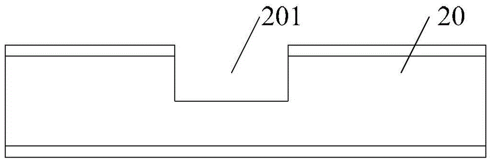
[0025] like figure 2 Shown is a schematic diagram of the circuit board 20 in the embodiment of the present invention. The circuit board 20 has a stepped groove 201. The groove bottom of the stepped groove 201 can be processed or not processed according to actual needs. The circuit board 20 can be produced by conventional processing methods, such as blanking, inner layer graphics, lamination, drilling, slotting, outer layer graphics and other steps.

[0026] 120. Make a spacer, the size of which matches the step groove, and the spacer is provided with the same hollow figure as the design figure at the bottom of the step groove.

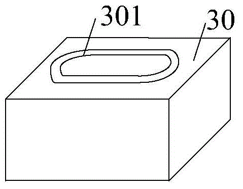
[0027] like image 3 As shown, it is a schematic diagram of the spacer 30 made in the embodiment of the present invention. The size...


PUM


Abstract

The invention discloses an exposure development method for a circuit board and solves problems of deficient exposure, poor graph precision and poor graph uniformity existing during groove bottom graph exposure in the prior art. The method comprises steps that, a circuit board having a step groove is provided; a pad is made, the size of the pad is in matching with the step groove, and the pad is provided with a hollowed-out graph identical to a design graph of the bottom of the step groove; the circuit board is coated with a photosensitive material, and the photosensitive material covers the bottom of the step groove; the pad is arranged in the step groove, exposure of the circuit board is carried out, and exposure of the photosensitive material coated at the bottom of the step groove is realized through the hollowed-out graph; the pad is taken out, development of the photosensitive material on the circuit board is carried out, and the required graph is formed on the circuit board.

Description

technical field [0001] The invention relates to the technical field of circuit boards, in particular to an exposure and development method for circuit boards. Background technique [0002] At present, more and more circuit boards are designed with partial three-dimensional structures, such as stepped grooves. In order to achieve specific functions, some circuit boards also need to process graphics on the bottom of the stepped groove, such as solder mask graphics. [0003] The conventional solder resist processing method includes the following steps: After coating the solder resist on the surface of the circuit board including the groove bottom of the step groove, placing the negative film on the surface of the circuit board, and then performing exposure and development to realize the transfer of the graphics on the negative film to the circuit board Finally, the solder resist pattern formed on the surface of the circuit board and the bottom of the stepped groove is cured to...

Claims


Application Information

Patent Timeline
Patent Type & Authority Applications(China)
IPC IPC(8): H05K3/00
Inventor 王蓓蕾张文梅谢占昊缪桦
Owner SHENNAN CIRCUITS
Learn More