Chip layout structure and method for preventing latch up effects and noise interference

A technology of noise interference and latch-up effect, applied in electrical components, electric solid-state devices, circuits, etc., can solve problems such as increasing the layout area, and achieve the effect of improving work performance, preventing latch-up effect, and good anti-latch effect.

Inactive Publication Date: 2016-05-04
WUHAN XINCHANG TECH CO LTD
View PDF5 Cites 6 Cited by
  • Summary
  • Abstract
  • Description
  • Claims
  • Application Information

AI Technical Summary

Problems solved by technology

For noise, it is mainly digital modules and high-frequency modules that will generate noise that interferes with analog modules. ), and increase the distance between the digital module and other modules to prevent noise interference, which will also increase the layout area

Method used


Image

  • Chip layout structure and method for preventing latch up effects and noise interference
  • Chip layout structure and method for preventing latch up effects and noise interference
  • Chip layout structure and method for preventing latch up effects and noise interference

Examples


Embodiment Construction

[0017] Below in conjunction with accompanying drawing, technical scheme of the present invention is described in further detail:

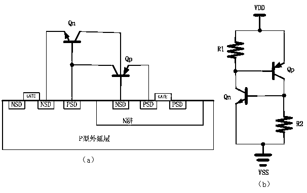
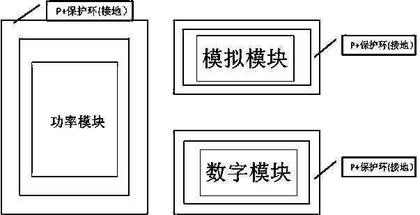
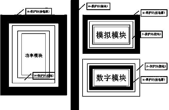
[0018] like image 3 As shown, the present invention provides a chip layout structure for preventing latch-up effect and noise interference. The chip layout includes an analog module, a power module, and a digital module. The analog module, the power module, and the digital module all adopt a double-ring protection structure, wherein, The double-ring protection structure of the analog module and the power module is the inner P+ ring (grounded), the outer N+ ring (connected to the power supply), the double-ring protection structure of the digital module is the inner N+ ring (connected to the power supply), the outer P+ ring (grounded), and the analog Keep a certain distance between the module and the digital module to prevent digital noise from interfering with the analog module. There is also an N+ minority carrier protection ring between the powe...


PUM


Abstract

The invention discloses a chip layout structure and a method for preventing latch up effects and noise interference. Dual-ring protection is adopted, an analog module of the chip is wrapped by firstly using a P+ring (is grounded) and then using an N+ring (is connected with a power supply); a power module is protected by using the dual-ring structure which is the same as the analog module; and a digital module is wrapped by firstly using the N+ring (is connected with the power supply) and then using the P+ring (is grounded). A certain distance is kept between the analog module and the digital module for preventing the analog module from being disturbed by digital noise. An N+ (minority carrier) protection ring is added between the power module and other modules, the N+ring is connected with a ground potential, the concentration of a substrate close to the minority carrier ring is reduced, substrate resistance is added, the latch up effects can be prevented from happening to the chip, and noise of the digital module can be prevented from disturbing the power module. Effects of good anti-latch up effects and noise isolation can be generated, and the working performance of the chip is improved.

Description

technical field [0001] The invention relates to a chip layout structure and method for preventing latchup effect latchup and noise interference, and belongs to the technical field of integrated circuits. Background technique [0002] With the development of the IC manufacturing process, the size of the chip is getting smaller and smaller, and the chip packaging density and integration are getting higher and higher, the possibility of latchup will become more and more likely, and the possibility of mutual interference between modules will also increase. bigger and bigger. Generally speaking, the conditions for generating latchup are: the loop current gain is greater than 1, βnpn*βpnp>=1; both BJT emitters are in forward bias; a current larger than the PNPN device maintenance current can be formed at the emitter. Due to the large current in the output stage of the power module, a certain displacement current will be generated in the substrate close to the power device. Whe...

Claims


Application Information

Patent Timeline
Patent Type & Authority Applications(China)
IPC IPC(8): H01L27/02H01L21/70
CPCH01L27/0207H01L21/70
Inventor 曾庆沈磊李玮
Owner WUHAN XINCHANG TECH CO LTD
Why Eureka
Try Eureka