

Film-forming mask and touch panel substrate
A film forming and masking technology, applied in ion implantation plating, conductive layer on insulating carrier, coating, etc., can solve the problems of poor film pattern position accuracy, film wrinkle, warpage, etc., and achieve improved position Accuracy, effect of suppressing deformation
- Summary
- Abstract
- Description
- Claims
- Application Information
AI Technical Summary
Problems solved by technology
Method used
Image

Examples
Embodiment Construction
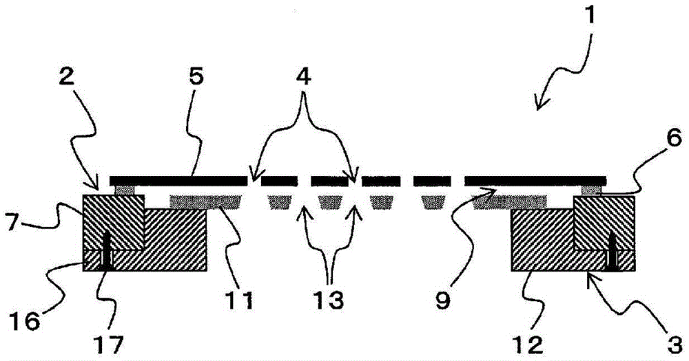
[0019] Embodiments of the present invention will be described in detail below with reference to the accompanying drawings. figure 1 It is a centerline cross-sectional view showing an embodiment of the film formation mask according to the present invention. This film formation mask 1 is used to form a thin film pattern on a substrate, and is configured to include a first mask 2 and a second mask 3 .
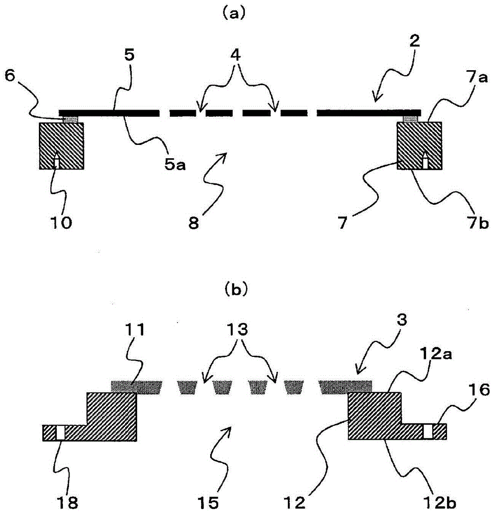
[0020] The above-mentioned first mask 2 is used to form a film on the substrate through the opening pattern 4 to form a thin film pattern, and is a mask to be a main mask, such as figure 2 As shown in (a), it is configured to include a resin film (hereinafter referred to as “resin mask 5 ”), a metal thin film 6 , and a first frame 7 .
[0021] Here, the above-mentioned resin mask 5 corresponds to a plurality of thin film patterns formed on the substrate, and is formed with a plurality of penetrating opening patterns 4 having the same shape and size as the thin film patterns, for...
PUM
 Abstract
Description
Claims
Application Information