Secondary-etching double-sided circuit board and processing technology thereof

A double-sided circuit board and secondary etching technology, which is applied to printed circuit components, chemical/electrolytic methods to remove conductive materials, etc., can solve the problems of uncontrolled product quality, long cycle time, and high cost investment. , to achieve the effect of simplifying the production process and operation difficulty, reducing the cost of PCB production, and reducing the investment of human resources

Active Publication Date: 2016-05-11
苏州市三生电子有限公司
View PDF5 Cites 2 Cited by
  • Summary
  • Abstract
  • Description
  • Claims
  • Application Information

AI Technical Summary

Problems solved by technology

[0002] In the current circuit board processing technology, double-sided circuit boards with GTL circuit layer, GBL internal circuit layer and GBL external circuit layer are all manufactured three times, and the circuit production is completed one by one. The cumulative error of production is very large, and the product quality is high. Without control, the operation cycle is long, the production cycle is long, the production delivery time cannot be improved, and the cost investment is also large, which cannot meet customer requirements; the operation can be completed after the second research, and the product quality can also be improved. be regulated

Method used


Image

  • Secondary-etching double-sided circuit board and processing technology thereof
  • Secondary-etching double-sided circuit board and processing technology thereof
  • Secondary-etching double-sided circuit board and processing technology thereof

Examples


Embodiment Construction

[0027] Below in conjunction with accompanying drawing and embodiment the present invention is described in further detail:

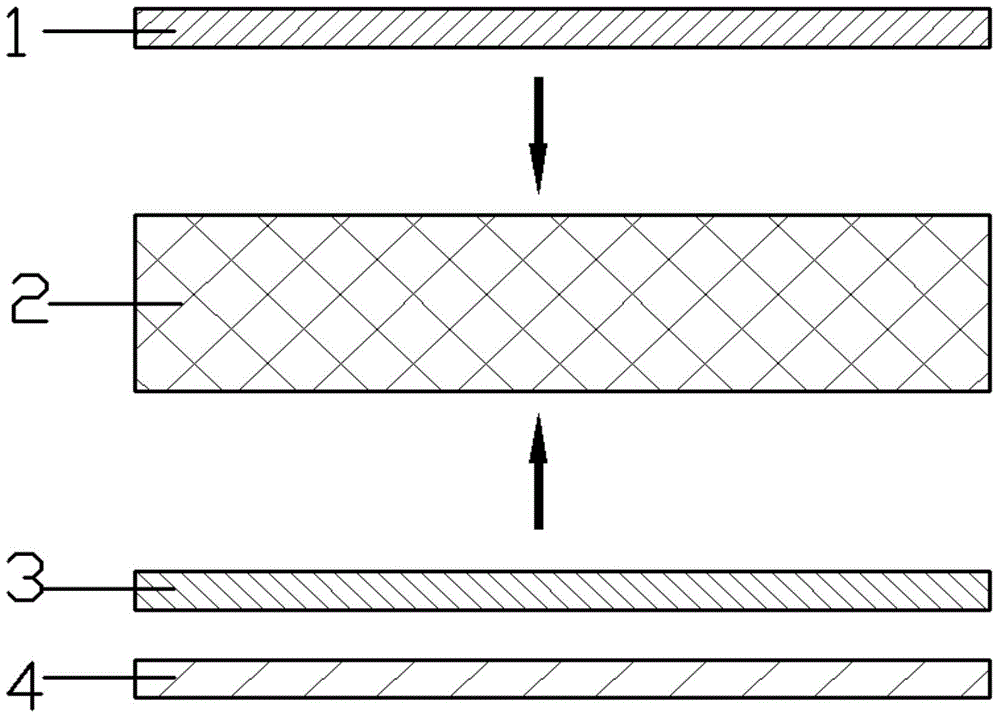
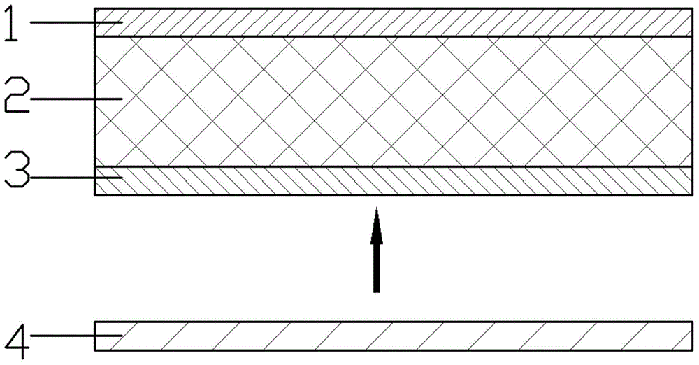
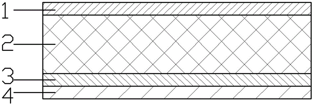
[0028] refer to image 3 As shown, a double-sided circuit board is etched twice, comprising: GTL line layer 1, insulating PP layer 2 and GBL step surface line layer, and the GBL step surface line layer is composed of GBL inner line layer 3 and GBL outer line layer 4 Composition, the GTL line layer 1 and the GBL inner line layer 3 are connected to the insulating PP layer 2 at the same time, the GBL outer line layer 4 covers the GBL inner line layer 3, the GBL outer line layer 4 and the GBL inner line layer 3 has similar appearance and shape, but the size of GBL outer circuit layer 4 is 0.05mm larger than the size of GBL inner circuit layer 3,

[0029] The processing technology of the second etching double-sided circuit board: includes the sub-flow of the first circuit manufacturing process and the second sub-flow of the circuit manufacturing process.

...


PUM


Abstract

The invention discloses a secondary-etching double-sided circuit board and a processing technology thereof. The secondary-etching double-sided circuit board comprises a GTL line layer, an insulation PP layer and a GBL step surface line layer. The GBL step surface line layer is formed by a GBL inner line layer and a GBL outer line layer. The GTL line layer and the GBL inner line layer are simultaneously connected to the insulation PP layer. The GBL outer line layer covers the GBL inner line layer. The secondary-etching double-sided circuit board processing technology comprises the following steps of first line making; line development cam compensation; line inspection; etching; second line making; line development cam compensation; line inspection; etching; open-short-circuit electric measurement; back-end processing. In the invention, second making is only needed, an investment is less, a production process and working difficulty are simplified, production efficiency is increased, production cost is reduced, a reject ratio of a product is decreased and a production period of the product is shortened.

Description

technical field [0001] The invention relates to a circuit board and its processing technology, in particular to a secondary etching double-sided circuit board and its processing technology. Background technique [0002] In the current circuit board processing technology, double-sided circuit boards with GTL circuit layer, GBL internal circuit layer and GBL external circuit layer are all manufactured three times, and the circuit production is completed one by one. The cumulative error of production is very large, and the product quality is high. Without control, the operation cycle is long, the production cycle is long, the production delivery time cannot be improved, and the cost investment is also large, which cannot meet customer requirements; the operation can be completed after the second research, and the product quality can also be improved. get regulated. In order to solve the above problems, a new type of superimposed circuit board circuit production update technolo...

Claims


Application Information

Patent Timeline
Patent Type & Authority Applications(China)
IPC IPC(8): H05K1/02H05K3/06
Inventor 孙祥根
Owner 苏州市三生电子有限公司
Why Eureka
Try Eureka