Supercharge Your Innovation With Domain-Expert AI Agents!

Data correction device, drawing device, inspection device, data correction method, drawing method, inspection method, and recording medium

A technology for data correction and design data, applied in image data processing, instruments, electrical components, etc., can solve the problem that etching correction takes a long time, etc.

Active Publication Date: 2018-05-25
DAINIPPON SCREEN MTG CO LTD
View PDF8 Cites 0 Cited by
  • Summary
  • Abstract
  • Description
  • Claims
  • Application Information

AI Technical Summary

Problems solved by technology

In this case, it is conceivable to obtain etching characteristics for each part and perform data correction (etching correction) based on the etching characteristics, but it takes a long time to perform etching correction for all parts.

Method used


Image

  • Data correction device, drawing device, inspection device, data correction method, drawing method, inspection method, and recording medium
  • Data correction device, drawing device, inspection device, data correction method, drawing method, inspection method, and recording medium
  • Data correction device, drawing device, inspection device, data correction method, drawing method, inspection method, and recording medium

Examples


Embodiment Construction

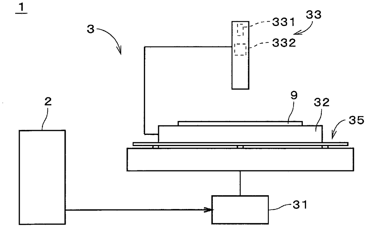
[0034] figure 1 It is a diagram showing the configuration of the drawing device 1 according to the first embodiment of the present invention. The drawing device 1 draws a circuit directly on a resist film by irradiating light to a resist film which is a photosensitive material provided on the surface of a printed board, a semiconductor substrate, a liquid crystal substrate, etc. (hereinafter simply referred to as "substrate 9"). Device for directly drawing images such as patterns. The substrate 9 on which the pattern is drawn by the drawing device 1 is developed and etched in a substrate processing device or the like (not shown). Thus, a pattern is formed on the substrate 9 . The etching of the substrate 9 is, for example, wet etching performed by applying an etchant to the substrate 9 . In addition, as the etching of the substrate 9, for example, dry etching using plasma or the like may be performed.

[0035] The drawing device 1 includes a data processing device 2 and an...


PUM


Abstract

The invention relates to a data correcting apparatus, a drawing apparatus, an inspection apparatus, a data correcting method, a drawing method, an inspection method and a recording medium. The etching characteristic storage part of the data correcting apparatus stores the etching characteristic of each of a plurality of object positions on an object as an object etching characteristic. A characteristic set acquisition part divides the plurality of object positions into a specific number of characteristic groups through storing the object positions which correspond with mutually similar object etching characteristics into one characteristic group, wherein the specific number is smaller than the number of the plurality of object positions. A dividing data correction part divides designing data of a pattern which is formed on the object through etching to a plurality of divided data that correspond with the plurality of dividing areas on the object. Furthermore each divided data are corrected based on the etching characteristic which represents one characteristic group affliated to an object position that is closest to the dividing area that corresponds with the divided data. Therefore, high-precision etching correction can be performed.

Description

technical field [0001] The present invention relates to a technique for correcting design data of a pattern formed on an object by etching. Background technique [0002] Conventionally, in the manufacturing process of semiconductor substrates, printed circuit boards, or glass substrates for plasma display devices or liquid crystal display devices (hereinafter referred to as "substrates"), various treatments are performed on the substrates. For example, a wiring pattern is formed on a substrate by etching a substrate having a resist pattern formed on its surface. In this etching, the shape of the pattern formed on the substrate may differ from the design data due to the density of the pattern arrangement, the size of the pattern, and the like. [0003] Japanese Patent No. 3074675 discloses a technique in which a resist pattern is formed on a substrate by using an electron beam direct drawing device, and then etched by a plasma etching device to form the pattern. In addition...

Claims


Application Information

Patent Timeline
Patent Type & Authority Patents(China)
IPC IPC(8): H01L21/66H01L21/67G06T7/00
CPCG06T7/0006G06T2207/10004G06T2207/30141H01L21/67063H01L22/12H01L22/20
Inventor 山田亮
Owner DAINIPPON SCREEN MTG CO LTD
Features
  • R&D
  • Intellectual Property
  • Life Sciences
  • Materials
  • Tech Scout
  • Unparalleled Data Quality
  • Higher Quality Content
  • 60% Fewer Hallucinations
Learn More