Pixel circuit and driving method thereof, display panel

A pixel circuit and non-driving technology, applied in static indicators, instruments, etc., can solve problems such as failure of threshold voltage compensation function, increased threshold voltage drift of driving transistors, and poor display effect of organic light-emitting diode display devices, etc., to achieve extended Effects of service life, increased service life, and reduced threshold voltage drift

Active Publication Date: 2016-05-25
BOE TECH GRP CO LTD
6 Cites 46 Cited by

AI-Extracted Technical Summary

Problems solved by technology

[0003] However, during the display process of the organic light emitting diode display device, the gate-source voltage is continuously applied between the gate and the source of the driving transistor of each pixel, so the threshold voltage drift of the driving transistor of each pixel will continue to increase
When the threshold voltage drift is within a certain range, the threshold voltage drift can be compensa...

Abstract

The invention discloses a pixel circuit and a driving method thereof, a display panel including the pixel circuit. The pixel circuit is composed of a light emitting module, a first driving module and a second driving module. The first driving module drives the light emitting module to emit light at a first period under the control of a first scanning signal from a first scanning control terminal; and the second driving module drives the light emitting module to emit light at a second period under the control of a second scanning signal from a second scanning control terminal, wherein the first period and the second period are not overlapped. Because the two driving modules drive the light emitting module alternately to emit light, one driving module enters a recovery stage when the other driving module drives the light emitting module to emit light, so that threshold voltage drifting of driving transistors of all driving modules can be reduced; and service lives of f driving transistors of all driving modules can be prolonged.

Application Domain

Static indicating devices

Technology Topic

EngineeringRecovery stage +2

Image

  • Pixel circuit and driving method thereof, display panel
  • Pixel circuit and driving method thereof, display panel
  • Pixel circuit and driving method thereof, display panel

Examples

  • Experimental program(1)

Example Embodiment

[0033] In order to make the objectives, technical solutions and advantages of the embodiments of the present invention more obvious, the exemplary embodiments of the present invention will be described in detail below with reference to the accompanying drawings. Obviously, the described example embodiments are only a part of the embodiments of the present invention, rather than all the embodiments of the present invention. All other embodiments obtained by those skilled in the art without creative work should fall into this Within the scope of protection of the invention.
[0034] Here, it should be noted that in the drawings, the same reference numerals are given to constituent parts that basically have the same or similar structure and function, and repeated descriptions about them will be omitted.
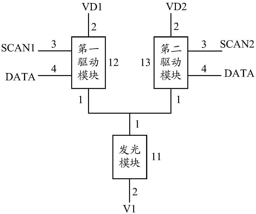
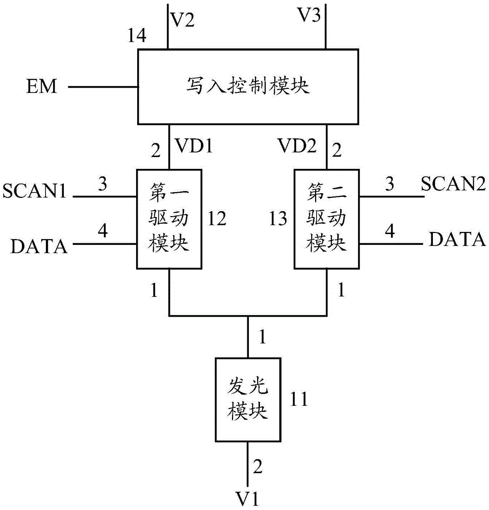
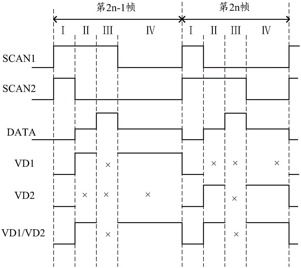
[0035] figure 1 It is a schematic block diagram of a pixel circuit according to an embodiment of the present invention. Such as figure 1 As shown, the pixel circuit according to the embodiment of the present invention includes a light emitting module 11, a first driving module 12, and a second driving module 13.
[0036] The first terminal 1 of the light-emitting module 11 is connected to the first terminal 1 of the first driving module 12 and the first terminal 1 of the second driving module 13, and the second terminal 2 thereof is connected to the first power voltage terminal V1.
[0037] The second terminal 2 of the first driving module 12 is connected to the first driving voltage terminal VD1, the third terminal 3 is connected to the first scan control terminal SCAN1, and the fourth terminal 4 is connected to the data input terminal DATA. The first driving module 12 is configured to drive the light emitting module 11 to emit light during a first period of time under the control of the first scan signal of the first scan control terminal SCAN1.
[0038] The second terminal 2 of the second driving module 13 is connected to the second driving voltage terminal VD2, the third terminal 3 is connected to the second scan control terminal SCAN2, and the fourth terminal 4 is connected to the data input terminal DATA. The second driving module 13 is configured to drive the light emitting module 11 to emit light during the second period under the control of the second scan signal of the second scan control terminal SCAN2. The first period and the second The time periods do not overlap with each other.
[0039] The first driving module 12 and the second driving module 13 alternately drive the light emitting module 11 to emit light.
[0040] According to the embodiment of the present invention, the duration of the first period and the second period are equal, and both may be one frame, two frames, multiple frames or any suitable period. For example, the first period may be an odd frame, and the second period may be an even frame, that is, the first driving module 12 may drive the light emitting module 11 to emit light during the odd frame, and the second driving module 13 may The light emitting module 11 is driven to emit light during the even number of frames. For another example, the first period may be an even-numbered frame, and the second period may be an odd-numbered frame, that is, the first driving module 12 may drive the light-emitting module 11 to emit light during the even-numbered frame, and the second driving module 13 The light emitting module 11 can be driven to emit light during an odd number of frames.
[0041] According to the embodiment of the present invention, during the first period of time when the first driving module 12 drives the light emitting module 11 to emit light, the second driving module 13 is in the recovery phase; while the second driving module 13 drives During the second time period when the light-emitting module 11 emits light, the first driving module 12 is in the recovery phase.
[0042] By making the first driving module 12 and the second driving module 13 alternately drive the light-emitting module 11 to emit light, and the second driving module 13 is in the recovery phase and during the second driving period when the first driving module 12 drives the light-emitting module 11 to emit light. The module 13 drives the light-emitting module 11 to emit light while the first driving module 12 is in the recovery phase. The driving transistor in each driving module of the first driving module 12 and the second driving module 13 can enter the recovery period after a period of operation, thereby reducing The threshold voltage of the driving transistor in each of the first driving module 12 and the second driving module 13 is shifted, so that the service life of the display panel can be prolonged.
[0043] figure 2 It is another schematic block diagram of a pixel circuit according to an embodiment of the present invention. Such as figure 2 As shown, the pixel circuit according to the embodiment of the present invention further includes a writing control module 14.
[0044] The first terminal of the write control module 14 is connected to the second power supply voltage terminal V2, the second terminal is connected to the third power supply voltage terminal V3, the third terminal is connected to the write control terminal EM, and the fourth terminal serves as The fifth terminal of the first driving voltage terminal VD1 serves as the second driving voltage terminal VD2.
[0045] The write control module 14 is configured to: under the control of the write control signal of the write control terminal EM, according to the second power supply voltage signal of the second power supply voltage terminal V2 and the third power supply voltage The third power supply voltage signal at the terminal V3 generates the first driving voltage signal at the first driving voltage terminal VD1 and the second driving voltage signal at the second driving voltage terminal VD2.
[0046] Hereinafter, the pixel circuit according to the embodiment of the present invention will be introduced by taking the first period as an odd frame and the second period as an even frame as an example.
[0047] According to the embodiment of the present invention, during the odd-numbered frame, under the control of the first scan signal of the first scan control terminal SCAN1 and the first driving voltage signal of the first driving voltage terminal VD1, the first driving module 12 can read the data signal of the data input terminal DATA and drive the light-emitting module 11 to emit light according to the read data signal, and during the even-numbered frame, the first driving module 12 is reset and is in the recovery stage.
[0048] According to the embodiment of the present invention, during the odd-numbered frame, the second driving module 13 is reset and in the recovery phase, and during the even-numbered frame, the second scan signal of the second scan control terminal SCAN2 and the first Under the control of the second driving voltage signal of the second driving voltage terminal VD2, the second driving module 13 reads the data signal of the data input terminal DATA and drives the light emitting module 11 to emit light according to the read data signal.
[0049] According to an embodiment of the present invention, each frame may be divided into a reset period, a compensation period, a data writing period, and a light emitting period.
[0050] During the odd-numbered frame (the (2n-1)th frame), in the reset period, the first driving module 12 and the second driving module 13 are both reset; in the compensation period, the first driving module 12 Under the action of the first scan control signal of the first scan control terminal SCAN1 and the first drive voltage signal of the first drive voltage terminal VD1, compensate the threshold voltage drift of the driving transistor in the first driving module 12; In the data writing period, the first driving module 12 reads all data under the action of the first scan control signal of the first scan control terminal SCAN1 and the first driving voltage signal of the first driving voltage terminal VD1. The data signal of the data input terminal DATA; in the light-emitting period, the first driving module 12 drives the light-emitting module 11 to emit light according to the read data signal; and in the compensation period, the data writing period and the light-emitting period, the The second driving module 13 maintains the reset state to be in the recovery phase.
[0051] During the even-numbered frame (the (2n)th frame), in the reset period, the first driving module 12 and the second driving module 13 are both reset; in the compensation period, the second driving module 13 is Under the action of the second scan control signal of the second scan control terminal SCAN2 and the second drive voltage signal of the second drive voltage terminal VD2, the threshold voltage drift of the drive transistor in the second drive module 13 is compensated; During the writing period, the second drive module 13 reads the data under the action of the second scan control signal of the second scan control terminal SCAN2 and the second drive voltage signal of the second drive voltage terminal VD2 The data signal of the input terminal DATA; in the light-emitting period, the second driving module 13 drives the light-emitting module 11 to emit light according to the read data signal; and in the compensation period, the data writing period, and the light-emitting period, the first The drive module 12 maintains the reset state to be in the recovery phase.
[0052] image 3 It is a schematic timing diagram of the signals of each signal terminal of the pixel circuit in each working period according to the embodiment of the present invention. in image 3 In, the reset period, the compensation period, the data writing period, and the light emission period are denoted as I, II, III, and IV, respectively.
[0053] According to the embodiment of the present invention, in the reset period I of each frame, the first driving voltage terminal VD1 and the second driving voltage terminal VD2 both output a non-driving voltage; during the odd-numbered frame, during the data writing period, The first driving voltage terminal VD1 is floating and there is no voltage output; in the compensation period and the light emitting period, the first driving voltage terminal VD1 outputs the driving voltage; during the even-numbered frame, in the data writing period, the The second driving voltage terminal VD2 is floating and has no voltage output; during the compensation period and the light emitting period, the second driving voltage terminal VD2 outputs a driving voltage. Optionally, the second driving voltage terminal VD2 is the same as the first driving voltage terminal VD1 (eg image 3 In VD1/VD2), the third power supply voltage terminal V3 is the same as the second power supply voltage terminal V2. In this case, in the reset period I of each period of the first period and the second period, the non-driving voltage is output at the first driving voltage terminal VD1; in the data writing period, the first driving voltage terminal VD1 Floating and no voltage output; during the compensation period and the light-emitting period, the first driving voltage terminal VD1 outputs a driving voltage.
[0054] Alternatively, optionally, the second driving voltage terminal VD2 is different from the first driving power terminal VD1, and the third power voltage terminal V3 is the same as or different from the second power voltage terminal V2. In this case, during the reset period of the odd frame and the even frame, the first driving voltage terminal VD1 and the second driving voltage terminal VD2 both output the non-driving voltage; during the odd frame, during the compensation period, the data writing In the input period and the light emission period, the second driving voltage terminal VD2 floats or outputs a non-driving voltage. In the data writing period, the first driving voltage terminal VD1 floats and no voltage is output. During the period and the light-emitting period, the first driving voltage terminal VD1 outputs the driving voltage; during the even-numbered frame, in the compensation period, the data writing period and the light-emitting period, the first driving voltage terminal VD1 floats or outputs a non- The driving voltage. In the data writing period, the second driving voltage terminal VD2 is floating and no voltage is output, and in the compensation period and the light emitting period, the second driving voltage terminal VD2 outputs a driving voltage.
[0055] In addition, according to the embodiment of the present invention, during the odd-numbered frame, during the reset period I, the first scan signal of the first scan control terminal SCAN1 and the second scan signal of the second scan control terminal SCAN2 are both valid. In the compensation period II and the data writing period III, the first scan signal of the first scan control terminal SCAN1 is at an active level and the second scan signal of the second scan control terminal SCAN2 is at an inactive level; In the light-emitting period IV, the first scan signal of the first scan control terminal SCAN1 and the second scan signal of the second scan control terminal SCAN2 are both at an invalid level. During the even-numbered frame, in the reset period I, the first scan signal of the first scan control terminal SCAN1 and the second scan signal of the second scan control terminal SCAN2 are both effective levels; in the compensation period II and data In the writing period III, the first scan signal of the first scan control terminal SCAN1 is at an inactive level and the second scan signal of the second scan control terminal SCAN2 is at an effective level; in the light-emitting period IV, the The first scan signal of the first scan control terminal SCAN1 and the second scan signal of the second scan control terminal SCAN2 are both at an invalid level.
[0056] Figure 4 It is an example circuit diagram of the first driving module 12 and the second driving module 13 in the pixel circuit according to the embodiment of the present invention.
[0057] Such as Figure 4 As shown, the first driving module 12 includes a first switching transistor T1, a first driving transistor T2, and a first capacitor C1; the second driving module 13 includes a second switching transistor T3, a second driving transistor T4, and a second Capacitance C2.
[0058] The gate of the first switch transistor T1 serves as the third terminal of the first driving module 12 and is connected to the first scan control terminal SCAN1, and the first pole of the first switch transistor T1 serves as the first driver The fourth terminal of the module 12 is connected to the data input terminal DATA, and the second terminal of the first switching transistor T1 is connected to the gate of the first driving transistor T2 and the first terminal 1 of the first capacitor C1 .
[0059] The first electrode of the first driving transistor T2 is connected to the first driving voltage terminal VD1 as the second terminal of the first driving module 12, and the second electrode of the first driving transistor T2 is used as the first The first end of the driving module 12 is connected to the first end of the light emitting module 11 and the second end 2 of the first capacitor C1.
[0060] The gate of the second switch transistor T3 serves as the third terminal of the second driving module 13 and is connected to the second scan control terminal SCAN2, and the first pole of the second switch transistor T3 serves as the second driver. The fourth terminal of the module 13 is connected to the data input terminal DATA, and the second terminal of the second switch transistor T3 is connected to the gate of the second driving transistor T4 and the first terminal 1 of the second capacitor C2 .
[0061] The first electrode of the second driving transistor T4 serves as the second terminal of the second driving module 13 and is connected to the second driving voltage terminal VD2, and the second electrode of the second driving transistor T4 serves as the second terminal. The first end of the driving module 13 is connected to the first end of the light emitting module 11 and the second end 2 of the second capacitor C2.
[0062] According to an embodiment of the present invention, the light emitting module 11 may include an organic light emitting diode OLED.
[0063] As an example, the anode of the organic light emitting diode is used as the first terminal of the light emitting module 11, and the cathode of the organic light emitting diode is used as the second terminal of the light emitting module 11, and the first power supply voltage terminal V1 is the power source. Low voltage terminal.
[0064] Optionally, the first switching transistor T1, the first driving transistor T2, the second switching transistor T3, and the second driving transistor T4 are all N-type transistors, and the first pole and the second pole of each transistor are drains respectively. Pole and source. In this case, the non-driving voltage is a low voltage, the driving voltage is a high voltage; and the effective levels of the first and second scan signals are high, the first and second scan signals The invalid level of is low.
[0065] Alternatively, the first switching transistor T1, the first driving transistor T2, the second switching transistor T3, and the second driving transistor T4 are all P-type transistors, and the first electrode and the second electrode of each transistor are respectively source electrodes. And drain. In this case, the non-driving voltage is a low voltage, the driving voltage is a high voltage; and the effective levels of the first and second scanning signals are low, the first and second scanning signals The invalid level of is high.
[0066] Figure 5 It is an example circuit diagram of the write control module 14 according to an embodiment of the present invention.
[0067] Such as Figure 5 As shown in (A), the write control module 14 according to the embodiment of the present invention may include a fifth switch transistor T5. The gate of the fifth switch transistor T5 serves as the third terminal of the write control module 14 and is connected to the write control terminal EM, the first terminal is connected to the second power supply voltage terminal V2 (VDD), and the second The terminals serve as the first and second driving voltage terminals VD1 and VD2. In this case, the second power supply voltage terminal V2 and the third power supply voltage terminal V3 as described above are the same power supply voltage terminal VDD.
[0068] Optionally, the fifth switch transistor T5 is an N-type transistor, and its first electrode and second electrode are the drain and the source respectively. In this case, the effective level of the write control signal of the write control terminal EM is a high level, and the invalid level of the write control signal is a low level.
[0069] Alternatively, the fifth switch transistor T5 is a P-type transistor, and its first electrode and second electrode are the source and the drain respectively. In this case, the effective level of the write control signal of the write control terminal EM is a low level, and the invalid level of the write control signal of the write control terminal EM is a high level.
[0070] Such as Figure 5 As shown in (B), the write control module 14 according to the embodiment of the present invention may include a fifth switch transistor T5 and a sixth switch transistor T6. The gate of the fifth switch transistor T5 and the gate of the sixth switch transistor T6 are connected to the write control terminal EM as the third terminal of the write control module 14. The fifth switch transistor T5 The first pole of the fifth switch transistor T5 is connected to the second power supply voltage terminal V2 (VDD1), the second pole of the fifth switch transistor T5 serves as the first driving voltage terminal VD1, and the first pole of the sixth switch transistor T6 is The three power supply voltage terminals V3 (VDD2) are connected, and the second pole of the sixth switch transistor T6 serves as the second driving voltage terminal VD2.
[0071] Optionally, the fifth switch transistor T5 and the sixth switch transistor T6 are both N-type transistors, and the first electrode and the second electrode are drain and source respectively. In this case, the effective level of the write control signal of the write control terminal EM is a high level, and the invalid level of the write control signal is a low level.
[0072] Alternatively, the fifth switch transistor T5 and the sixth switch transistor T6 are both P-type transistors, and the first pole and the second pole are the source and the drain respectively. In this case, the effective level of the write control signal of the write control terminal EM is a low level, and the invalid level of the write control signal of the write control terminal EM is a high level.
[0073] Image 6 It is a schematic timing diagram of the signals of each signal terminal of the pixel circuit in each working period according to the embodiment of the present invention.
[0074] for Figure 5 In the write control module 14 shown in (A), in the reset period I, the compensation period II, and the light-emitting period IV, the write control signal of the write control terminal EM is at an effective level, and the fifth switch transistor T5 is turned on, and the power supply voltage signal of the power supply voltage terminal VDD is transmitted to the driving voltage terminal VD1/VD2; and in the data writing period III, the writing control signal of the writing control terminal EM is at an invalid level, so The fifth switch transistor T5 is turned off, and the driving voltage terminal VD1/VD2 is floated.
[0075] In addition, in the reset period I, the power supply voltage of the power supply voltage terminal VDD is the non-driving voltage; in the compensation period II and the light emission period IV, the power supply voltage of the power supply voltage terminal VDD is the driving voltage; in the data writing period III The power supply voltage of the power supply voltage terminal VDD may be a driving voltage or a non-driving voltage.
[0076] for Figure 5 In the write control module 14 shown in (B), during the odd-numbered frame (the (2n-1)th frame), the power supply voltages of the first power supply voltage terminal VDD1 and the second power supply voltage terminal VDD2 are non-driving voltages, In the compensation period II and the light emitting period IV, the power supply voltage of the first power supply voltage terminal VDD1 is the driving voltage; in the data writing period III, the power supply voltage of the first power supply voltage terminal VDD1 may be the driving voltage or non- Driving voltage; In the compensation period II, the data writing period III, and the light emitting period IV, the power supply voltage of the second power supply voltage terminal VDD2 may be a non-driving voltage or a driving voltage.
[0077] for Figure 5 In the write control module 14 shown in (B), during the even-numbered frame (the (2n)th frame), the power supply voltages of the first power supply voltage terminal VDD1 and the second power supply voltage terminal VDD2 are non-driving voltages. During period II and lighting period IV, the power supply voltage of the second power supply voltage terminal VDD2 is a driving voltage; in the data writing period III, the power supply voltage of the second power supply voltage terminal VDD2 may be a driving voltage or a non-driving voltage In the compensation period II, the data writing period III and the light emitting period IV, the power supply voltage of the first power supply voltage terminal VDD1 may be a non-driving voltage or a driving voltage.
[0078] Figure 7 It is an example circuit diagram of a pixel circuit according to an embodiment of the present invention. Such as Figure 7 The write control module in the pixel circuit shown is Figure 5 The write control module shown in (A).
[0079] Below, reference Image 6 as well as Figure 8 - Picture 11 Described as Figure 7 The driving method of the pixel circuit according to the embodiment of the present invention is shown.
[0080] During the odd frame period, under the control of the first scan signal of the first scan control terminal SCAN1, the first driving module 12 reads the data signal of the data input terminal DATA and drives according to the read data signal The light emitting module 11 emits light; under the control of the second scan signal of the second scan control terminal SCAN2, the second driving module 13 is reset and is in the recovery stage.
[0081] During the even-numbered frame, under the control of the second scan signal of the second scan control terminal SCAN2, the second drive module 13 reads the data signal of the data input terminal DATA and drives according to the read data signal The light emitting module 11 emits light; under the control of the first scan signal of the first scan control terminal SCAN1, the first driving module 12 is reset and is in the recovery stage.
[0082] Such as Image 6 As shown, each frame is divided into a reset period I, a compensation period II, a data writing period III, and a light emitting period IV. Figure 8 - Picture 11 This is an equivalent circuit diagram of the pixel circuit according to the embodiment of the present invention in each period during odd frames. Below, take the odd-numbered frame as an example to describe Figure 7 The illustrated operation of the pixel circuit according to the embodiment of the invention.
[0083] In the reset period I, the second power supply voltage terminal VDD is at the non-driving voltage Vss, the write control terminal EM is at an effective level, and the fifth switch transistor T5 in the write control module 14 is turned on, so The first driving voltage terminal VD1 and the second driving voltage terminal VD2 output the power supply voltage of the second power supply voltage terminal VDD, that is, the non-driving voltage Vss. In addition, in this period, the first scan signal of the first scan control terminal SCAN1 and the second scan signal of the second scan control terminal SCAN2 are both effective levels, and the first switch in the first drive module 12 The transistor T1 and the second switch transistor T3 in the second driving module 13 are turned on, and the data voltage Vss of the data input terminal DATA is transmitted to the gates of the first driving transistor T2 and the second driving transistor T4, and the first driving transistor T2 and the second driving transistor T4 are turned off to discharge the first capacitor C1 and the second capacitor C2, so that the voltage difference between the first capacitor C1 and the second capacitor C2 is zero. In this period, the gate-source voltage of the first driving transistor T2 and the second driving transistor T4 is zero, and the first driving transistor T2 and the second driving transistor T4 enter the recovery phase. In addition, during this period, the capacitance in the light-emitting module 11 (for example, the parasitic capacitance C3 of the light-emitting diode, hereinafter referred to as the third capacitance C3) is also discharged. The equivalent circuit diagram of the pixel circuit in this period according to the embodiment of the present invention is as follows: Figure 8 Shown. In this period, VA1=Vss, VA2=Vss, VB=Vss, and thus the first and second driving modules 12 and 13 are reset, and the light-emitting module 11 does not emit light.
[0084] In the compensation period II, the second power supply voltage terminal VDD is at the driving voltage Vdd, the write control terminal EM remains at an effective level, the fifth switch transistor T5 in the write control module 14 is turned on, and the The first driving voltage terminal VD1 and the second driving voltage terminal VD2 output the power supply voltage of the second power supply voltage terminal VDD, that is, the driving voltage Vdd. In addition, during this period, the first scan signal of the first scan control terminal SCAN1 is at an effective level, and the first switch transistor T1 in the first driving module 12 remains on, and the data at the data input terminal DATA The voltage Vref is transmitted to the gate of the first driving transistor T2, Vref-Vss> Vth2, Vth2 are the threshold voltages of the first drive transistor T2, the first drive transistor T2 is turned on, and the third capacitor C3 is charged; the second scan signal of the second scan control terminal SCAN2 is at an invalid level , The second switching transistor T3 in the second driving module 13 is turned off, and the second driving transistor T4 is kept turned off, that is, the second driving module 13 is kept in a reset state. When entering the compensation period II, VA1=Vref, VB=Vss, and Vgs2=Vref-Vss> Vth2, where Vgs2 is the gate-source voltage of the first driving transistor T2, so the first driving transistor T2 is turned on. As the third capacitor C3 is charged, the voltage VB at point B rises. When VB rises to Vref-Vth2, the first drive transistor T2 is turned off, so the voltage stored on both ends of the first capacitor C1 is VC1=VA1 -VB=Vref-(Vref-Vth2)=Vth2. The equivalent circuit diagram of the pixel circuit in this period according to the embodiment of the present invention is as follows: Picture 9 Shown. At the end of this period, VA1=Vref, VB=Vref-Vth2, VC1=Vth2, so the first capacitor C1 stores the threshold voltage of the first driving transistor T2, that is, the first driving module 12 performs the first driving transistor The threshold voltage of T2 is compensated, and the light-emitting module 11 does not emit light.
[0085] In the data writing period III, the second power supply voltage terminal VDD is at the driving voltage Vdd or the non-driving voltage Vss, the writing control terminal EM is at an invalid level, and the fifth switch in the writing control module 14 The transistor T5 is turned off, and the first driving voltage terminal VD1 and the second driving voltage terminal VD2 float. In addition, during this period, the first scan signal of the first scan control terminal SCAN1 is at an effective level, and the first switch transistor T1 in the first driving module 12 remains on, and the data at the data input terminal DATA The voltage Vdata is transferred to the gate of the first driving transistor T2, Vdata-VB=Vdata-(Vref-Vth2)=Vth2+(Vdata-Vref)> Vth2, the first drive transistor T2 is turned on; the second scan signal of the second scan control terminal SCAN2 is at an inactive level, the second switch transistor T3 in the second drive module 13 remains turned off, and the second drive The transistor T4 remains off, that is, the second driving module 13 remains in the reset state. During this period, although the first driving transistor T2 is turned on, because the first driving voltage terminal VD1 is floating, the voltage at point B is determined by the capacitance of the first capacitor C1 and the third capacitor C3, so the third capacitor C3 is charged Upon completion, VB=(Vref-Vth2)+a1(Vdata-Vref), where a1=C1/(C1+C3). The equivalent circuit diagram of the pixel circuit in this period according to the embodiment of the present invention is as follows: Picture 10 Shown. At the end of this period, VA1=Vdata, VB=(Vref-Vth2)+a1(Vdata-Vref), Vgs2=VA1-VB=(1-a1)(Vdata-Vref)+Vth2, thus the first capacitor C1 The threshold voltage Vth2 of the first driving transistor T2 and the data signal Vdata of the data input terminal DATA are stored, that is, the first driving module 12 reads in the data signal Vdata of the data input terminal DATA, and the light emitting Module 11 does not emit light.
[0086] In the light-emitting period IV, the second power supply voltage terminal VDD is at the driving voltage Vdd, the write control terminal EM is at an effective level, the fifth switch transistor T5 in the write control module 14 is turned on, and the first A driving voltage terminal VD1 and a second driving voltage terminal VD2 output the power supply voltage of the second power supply voltage terminal VDD, that is, the driving voltage Vdd. In addition, during this period, the first scan signal of the first scan control terminal SCAN1 is at an inactive level, the first switch transistor T1 in the first driving module 12 is turned off, and the first capacitor C1 maintains the voltage at both ends thereof. The first drive transistor T2 is turned on and drives the light-emitting module 11 to emit light; the second scan signal of the second scan control terminal SCAN2 is at an invalid level, and the second switch transistor T3 in the second drive module 13 remains off, The second driving transistor T4 remains turned off, that is, the second driving module 13 remains in a reset state. The equivalent circuit diagram of the pixel circuit in this period according to the embodiment of the present invention is as follows: Picture 11 Shown. In this period, the gate-source voltage of the first driving transistor T2 is maintained as Vgs2=(1-a1)(Vdata-Vref)+Vth2, so the first driving transistor T2 remains on and flows through the fifth driving transistor T5 , The current I of the first driving transistor T2 and the light-emitting device OLED Can be expressed as:
[0087] I O L E D = 1 2 · μ n · C o x · W 2 L 2 · ( V g s 2 - V t h 2 ) 2 = 1 2 · μ n · C o x · W 2 L 2 · [ ( 1 - a 1 ) ( V d a t a - V r e f ) ] 2 .
[0088] Among them, W2 and L2 are the channel width and length of the first driving transistor T2, μ n Is the effective carrier mobility, and Cox is the dielectric constant of the gate insulating layer.
[0089] It can be seen from the above formula that during odd frames, the current I flowing through the light-emitting device OLED It has nothing to do with the threshold voltage of the first driving transistor T2, but only with the data voltage Vref applied at the data input terminal during the compensation period and the data voltage Vdata applied at the data input terminal during the data writing period, thereby eliminating the drive transistor T2. The non-uniformity and drift of the threshold voltage affect the light-emitting brightness of the light-emitting device.
[0090] The operation of the pixel circuit according to the embodiment of the present invention during the odd frame is described above. Specifically, during the odd frame, the first driving module in the pixel circuit according to the embodiment of the present invention reads the data signal of the data input terminal DATA and The light emitting module is driven to emit light according to the read data signal, and the second driving module is reset and is in the recovery phase.
[0091] Similarly, during even-numbered frames, the second driving module in the pixel circuit according to the embodiment of the present invention reads the data signal of the data input terminal DATA and drives the light emitting module to emit light according to the read data signal, and the first driving module is Reset and in the recovery phase.
[0092] In the reset period I, the operation of the pixel circuit according to the embodiment of the present invention is the same as the operation in the reset period I during the odd-numbered frame, and will not be repeated here.
[0093] In the compensation period II, the second power supply voltage terminal VDD is at the driving voltage Vdd, the write control terminal EM remains at an effective level, the fifth switch transistor T5 in the write control module 14 is turned on, and the The first driving voltage terminal VD1 and the second driving voltage terminal VD2 output a driving voltage Vdd. In addition, during this period, the second scan signal of the second scan control terminal SCAN2 is at an effective level, the second switch transistor T3 in the second driving module 13 remains on, and the data input terminal DATA inputs a data voltage Vref, Vref-Vss> Vth4, where Vth4 is the threshold voltage of the second drive transistor T4 in the second drive module 13, the second drive transistor T4 is turned on, and the third capacitor C3 is charged; the first scan control terminal SCAN1 The scan signal is at an inactive level, the first switch transistor T1 in the first driving module 12 is turned off, and the first driving transistor T2 remains turned off, that is, the first driving module 12 remains in a reset state. When entering the compensation period II, VA2=Vref, VB=Vss, and the data voltage Vgs4=Vref-Vss> Vth4, where Vgs4 is the gate-source voltage of the first driving transistor T2, so the second driving transistor T4 is turned on. As the third capacitor C3 is charged, the voltage VB at point B rises. When VB rises to Vref-Vth4, the second drive transistor T4 is turned off, so the voltage stored on both ends of the second capacitor C2 is VC2=VA2 -VB=Vref-(Vref-Vth4)=Vth4. At the end of this period, VA2=Vref, VB=Vref-Vth4, so the second capacitor C2 stores the threshold voltage of the second driving transistor T4, that is, the second driving module 13 performs the threshold voltage of the second driving transistor T4 Compensation, and the light-emitting module 11 does not emit light.
[0094] In the data writing period III, the second power supply voltage terminal VDD is at the driving voltage Vdd or at the non-driving voltage Vss, the writing control terminal EM is at an invalid level, and the fifth switch in the writing control module 14 The transistor T5 is turned off, and the first driving voltage terminal VD1 and the second driving voltage terminal VD2 float. In addition, during this period, the second scan signal of the second scan control terminal SCAN2 is at an effective level, the second switch transistor T3 in the second driving module 13 remains on, and the data input terminal DATA inputs a data voltage Vdata, Vdata-VB=Vdata-(Vref-Vth4)=Vth4+(Vdata-Vref), the second driving transistor T4 is turned on; the first scan signal of the first scan control terminal SCAN1 is at an invalid level, The first switching transistor T1 and the first driving transistor T2 in a driving module 12 are kept off, that is, the first driving module 12 is kept in a reset state. In this period, when the third capacitor C3 is fully charged, the voltage at point B is determined by the capacitance of the second capacitor C2 and the third capacitor C3, VB=(Vref-Vth4)+a2(Vdata-Vref), where a2 =C2/(C2+C3). At the end of this period, VA2=Vdata, VB=(Vref-Vth4)+a2(Vdata-Vref), Vgs4=VA2-VB=(1-a2)(Vdata-Vref)+Vth4, thus the second capacitor C2 The threshold voltage Vth4 of the second driving transistor T4 and the data signal Vdata of the data input terminal DATA are stored, that is, the second driving module 13 reads in the data signal Vdata of the data input terminal DATA, and the light-emitting Module 11 does not emit light.
[0095] In the light-emitting period IV, the second power supply voltage terminal VDD is at the driving voltage Vdd, the write control terminal EM is at an effective level, the fifth switch transistor T5 in the write control module 14 is turned on, and the first A driving voltage terminal VD1 and a second driving voltage terminal VD2 output a driving voltage Vdd. In addition, during this period, the second scan signal of the second scan control terminal SCAN2 is at an inactive level, the second switch transistor T3 in the second driving module 13 is turned off, and the second capacitor C2 maintains the voltage at both ends thereof. The second driving transistor T4 is turned on and drives the light-emitting module 11 to emit light; the first scan signal of the first scan control terminal SCAN1 is at an invalid level, and the first switching transistor T1 in the first driving module 12 remains off, The first driving transistor T2 is kept off, that is, the first driving module 12 is kept in a reset state. In this period, the gate-source voltage of the second driving transistor T4 is maintained at Vgs4=(1-a2)(Vdata-Vref)+Vth4, so that the second driving transistor T4 remains on and flows through the fifth switching transistor T5 , The current I of the second driving transistor T4 and the light-emitting device OLED Can be expressed as:
[0096] I O L E D = 1 2 · μ n · C o x · W 4 L 4 · ( V g s 4 - V t h 4 ) 2 = 1 2 · μ n · C o x · W 4 L 4 · [ ( 1 - a 2 ) ( V d a t a - V r e f ) ] 2 .
[0097] Among them, W4 and L4 are the channel width and length of the second driving transistor T4, respectively.
[0098] It can be seen from the above formula that during the even number of frames, the current I flowing through the light-emitting device OLED It has nothing to do with the threshold voltage of the second driving transistor T4, but only with the data voltage Vref applied at the data input terminal during the compensation period and the data voltage Vdata applied at the data input terminal during the data writing period, thereby eliminating the drive transistor T4. The non-uniformity and drift of the threshold voltage affect the light-emitting brightness of the light-emitting device.
[0099] In order to keep the luminous brightness of the light emitting device at the same data voltage during the odd and even frames the same, the circuit structure can make the structural parameters of the first capacitor C1 and the second capacitor C2 exactly the same and make the first driving transistor T2 and The structural parameters of the second drive transistor T4 are exactly the same, that is, the capacitance values ​​of the first capacitor C1 and the second capacitor C2 are the same, and the channel parameters (width and length) of the first drive transistor T2 and the second drive transistor T4 are made the same.
[0100] The application according to the embodiment of the present invention is described above Figure 5 The operation of the pixel circuit of the writing control module 14 shown in (A) during odd and even frames, the application according to the embodiment of the present invention will be briefly described below Figure 5 The operation of the pixel circuit of the write control module 14 shown in (B) during the odd and even frames.
[0101] Such as Figure 5 As shown in (B), the second driving voltage terminal VD1 is different from the first driving voltage terminal VD2, and the third power supply voltage terminal VDD2 is the same as or different from the second power supply voltage terminal VDD1.
[0102] In the following, the application according to the embodiment of the present invention is first described Figure 5 (B) shows the operation of the pixel circuit of the write control module 14 during the odd-numbered frame period.
[0103] In the reset period I, the second power supply voltage terminal VDD1 and the third power supply voltage terminal VDD2 are both at the non-driving voltage Vss, the write control terminal EM is at an effective level, and the write control module 14 The fifth switching transistor T5 and the sixth switching transistor T6 are turned on, and the first driving voltage terminal VD1 and the second driving voltage terminal VD2 both output the non-driving voltage Vss. In addition, in this period, the first scan signal of the first scan control terminal SCAN1 and the second scan signal of the second scan control terminal SCAN2 are both effective levels, and the first switch in the first drive module 12 The transistor T1 and the second switch transistor T3 in the second driving module 13 are turned on, the data input terminal DATA inputs the data voltage Vss, and the first driving transistor T2 and the second driving transistor T4 are turned off. In this period, VA1=Vss, VA2=Vss, and VB=Vss.
[0104] In the compensation period II, the data writing period III, and the light emitting period IV, the fifth switch transistor T5 in the write control module 14, the first switch transistor T1 and the first drive transistor T2 in the first drive module 12 The operation and the above for the application according to the embodiment of the present invention Figure 5 The operation of the pixel circuit of the writing control module 14 shown in (A) during the odd-numbered frame period is the same, and will not be repeated here.
[0105] In addition, during the compensation period II, the data writing period III, and the light emitting period IV, the third power supply voltage terminal VDD2 may be a driving voltage or a non-driving voltage. The operation of the sixth switch transistor T6 in the writing control module 14 The operation of the fifth switching transistor T5 is the same, except that the second driving voltage terminal VD2 outputs the power supply voltage of the third power supply voltage terminal VDD2; in addition, the second switching transistor T3 in the second driving module 13 and the second driving The operation of the transistor T4 and the above for the application according to the embodiment of the present invention Figure 5 The operations of the second switch transistor T3 and the second drive transistor T4 in the pixel circuit of the writing control module 14 shown in (A) during the odd-numbered frame period are the same, and will not be repeated here.
[0106] The following briefly describes the application according to the embodiment of the present invention Figure 5 (B) shows the operation of the pixel circuit of the write control module 14 during the even-numbered frame.
[0107] In the reset period I, the application according to the embodiment of the present invention Figure 5 The operation of the pixel circuit of the writing control module 14 shown in (B) is the same as the operation of the reset period I during the odd-numbered frame, and will not be repeated here.
[0108] In the compensation period II, the data writing period III, and the light emitting period IV, the sixth switch transistor T6 in the write control module 14 and the second switch transistor T3 and the second drive transistor T4 in the second drive module 13 The operation and the above for the application according to the embodiment of the present invention Figure 5 The operation of the pixel circuit of the write control module 14 shown in (A) during the even-numbered frame period is the same, and will not be repeated here.
[0109] In addition, in the compensation period II, the data writing period III, and the light emitting period IV, the second power supply voltage terminal VDD1 may be a driving voltage or a non-driving voltage. The operation of the fifth switch transistor T5 in the writing control module 14 The operation is the same as that of the sixth switching transistor T5, except that the first driving voltage terminal VD1 outputs the power supply voltage of the second power supply voltage terminal VDD1; in addition, the first switching transistor T1 in the first driving module 12 and the first driving The operation of the transistor T2 and the above for the application according to the embodiment of the present invention Figure 5 The operations of the first switching transistor T1 and the first driving transistor T2 in the pixel circuit of the writing control module 14 shown in (A) during the even-numbered frame period are the same, and will not be repeated here.
[0110] Picture 12 It is a schematic block diagram of a display panel according to an embodiment of the present invention. Such as Picture 12 As shown, the display panel according to the embodiment of the present invention includes a pixel array, a gate drive circuit, and a data drive circuit, and each pixel in the pixel array includes the above-mentioned pixel circuit according to the embodiment of the present invention.
[0111] The gate driving circuit generates scan signals for each row of pixels in the pixel array. Specifically, for each row of pixels in the pixel array, the gate driving circuit generates the first scan signal and the second scan signal as described above, and the first scan signal is used to control the operation of the first driving module 12 , The second scan signal is used to control the operation of the second driving module 13.
[0112] The data driving circuit generates data signals for each column of pixels in the pixel array. Specifically, for each column of pixels in the pixel array, the data driving circuit generates the data signals Vss, Vref, and Vdata as described above in the reset period, compensation period, and data writing period of each frame, respectively.
[0113] According to the pixel circuit and the driving method thereof, and the display panel according to the embodiments of the present invention, the first driving module and the second driving module are used to alternately drive the light-emitting module to emit light, so that the second driving module is in the position when the first driving module drives the light-emitting module to emit light. During the recovery phase and during the period when the second driving module drives the light-emitting module to emit light, the first driving module is in the recovery phase, so that the driving transistors in each driving module can enter the recovery phase after a period of operation, thereby reducing the The threshold voltage of the driving transistor drifts, which can extend the service life of the display panel.
[0114] The various embodiments of the present invention are described in detail above. However, those skilled in the art should understand that various modifications, combinations or sub-combinations can be made to these embodiments without departing from the principle and spirit of the present invention, and such modifications should fall within the scope of the present invention.

PUM

no PUM

Description & Claims & Application Information

We can also present the details of the Description, Claims and Application information to help users get a comprehensive understanding of the technical details of the patent, such as background art, summary of invention, brief description of drawings, description of embodiments, and other original content. On the other hand, users can also determine the specific scope of protection of the technology through the list of claims; as well as understand the changes in the life cycle of the technology with the presentation of the patent timeline. Login to view more.

Similar technology patents

Operation method of OTS gate tube

PendingCN114284312AReduced Threshold Voltage DriftThe operation method is simple and controllable
Owner:HUAZHONG UNIV OF SCI & TECH +1

Glomerocryst cubic boron nitride composite sheet and preparation method for same

ActiveCN103158287AExtended service lifeIncreased depth of cut
Owner:ZHENGZHOU BERLT HARD MATERIALS

Sleep assistance mattress

ActiveCN106842979AReduce data processing pressureExtended service life
Owner:DONGGUAN UNIV OF TECH

Recovering and using technology of water in electroplating

Owner:海宁市海整整流器有限公司

Classification and recommendation of technical efficacy words

  • Reduced Threshold Voltage Drift
  • Extended service life

Operation method of OTS gate tube

PendingCN114284312AReduced Threshold Voltage DriftThe operation method is simple and controllable
Owner:HUAZHONG UNIV OF SCI & TECH +1

Fracturing manifold quick connecting device

Owner:YANTAI JEREH PETROLEUM EQUIP & TECH

Modified asphalt composition with creeping characteristic and preparation method thereof

InactiveCN102020859Aavoid rapid agingExtended service life
Owner:ZHEJIANG WOPUMAN HIGH NEW MATERIALS
Why Eureka
Try Eureka